

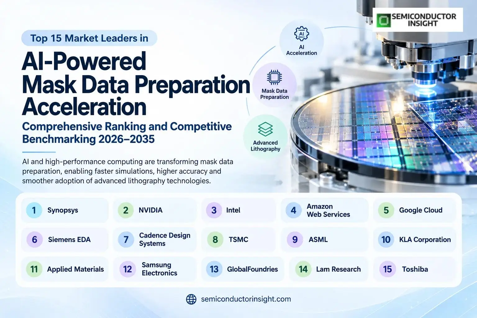
Top 15 Market Leaders in AI-Powered Mask Data Preparation Acceleration: Comprehensive Ranking and Competitive Benchmarking 2026–2035
AI-Powered Mask Data Preparation Acceleration Market sits at the intersection of semiconductor manufacturing, computational lithography, artificial intelligence and high-performance computing. Mask data preparation converts complex chip-layout information into the precise instructions required by photomask-writing equipment. Before those instructions reach manufacturing, the data may undergo fracture, mask rule checking, proximity correction, geometry processing and verification.
The growing complexity of advanced chips is making these operations increasingly demanding. Extreme ultraviolet (EUV) lithography, high-numerical-aperture EUV systems and curvilinear mask patterns require extensive calculations to predict how designed features will print on silicon. AI models and GPU acceleration can help reduce simulation time, prioritize computationally expensive regions and identify potential patterning problems earlier. However, AI-generated outputs still need to meet strict engineering and manufacturing requirements.
Synopsys: The Direct Mask Data Preparation Specialist
Synopsys stands apart from most companies on this list because mask data preparation is an established part of its semiconductor manufacturing software portfolio, rather than a potential application of general-purpose AI. Its MDP solutions support data fracture, mask rule checking, proximity-effect correction, job-deck processing, data sizing and verification. These operations convert intricate circuit layouts into machine-readable instructions for electron-beam, laser and multibeam mask-writing systems.
- Its SmartFracture, SmartMRC and mask error correction technologies address different stages of the preparation process.
- Synopsys also offers S-Litho simulation capabilities for evaluating pattern formation across DUV and EUV lithography.
- The company’s support for curvilinear mask data is particularly relevant as advanced chip designs require more sophisticated pattern shapes.
- For customers, the central advantage is the integration of data preparation, mask verification and lithography simulation within a specialized engineering environment.
NVIDIA: GPU Acceleration Brings Computational Lithography Into Focus
NVIDIA is one of the most consequential technology providers in this market because computational lithography relies on large-scale mathematical simulation. Its cuLitho library uses GPU acceleration to help semiconductor manufacturers perform optical proximity correction and inverse lithography calculations more efficiently. These workloads help engineers compensate for optical effects that would otherwise distort the patterns printed on silicon.
The October 2026 collaboration update between NVIDIA and Siemens provides a particularly strong industry example. The companies reported up to 12-fold acceleration for full-chip OPC workloads using cuLitho with Siemens Calibre, with selected simulation workloads achieving speed-ups of 10 to 17 times. The importance of these figures extends beyond faster processing: shorter runtimes can allow engineers to test more patterning alternatives, investigate difficult layouts and prepare advanced masks within tighter production schedules. NVIDIA is therefore an acceleration platform provider, not a replacement for the specialized software that validates mask data.
Intel AI: Advanced EUV Manufacturing Creates a Demanding Preparation Environment
Intel’s relevance comes from its role as both a semiconductor designer and a manufacturer working with increasingly advanced lithography processes. AI-based analysis, accelerated computing and manufacturing data can help identify patterning problems, optimize process conditions and support more efficient movement from chip design to production. These activities are closely related to the workloads that surround mask data preparation, although Intel is not principally an independent commercial MDP software vendor.
A major 2026 milestone came from Intel Foundry and ASML. In September, Intel reported that more than one million wafers had been processed across High-NA EUV tool certification, testing, research and development, and selected production layers. The milestone demonstrates that advanced lithography is progressing beyond equipment demonstrations into practical manufacturing activity.
For the wider market, this creates demand for increasingly precise mask data, reliable verification and computationally intensive pattern optimization. Intel’s significance lies in the real manufacturing environment that drives these requirements.
Amazon Web Services: Cloud Capacity for Large Semiconductor Workloads
Amazon Web Services (AWS) addresses one of the operational problems facing semiconductor engineering teams: the need to run computationally intensive workloads without permanently maintaining enough infrastructure for every peak-demand period. Its semiconductor design environment supports electronic design automation, verification, data management and cloud-based computing. These capabilities can support MDP and computational lithography when appropriate licensed engineering applications are deployed on the platform.
In August 2026, AWS published guidance on accelerating chip tape-out through AWS Unified Operations. The guidance addresses operational continuity, workload performance, security and cost management during demanding semiconductor development schedules. AWS also documents the use of scalable cloud resources for workflows ranging from design verification to fabrication-ready data delivery. For companies running extensive OPC or inverse lithography simulations, the attraction is the ability to provision computing and storage around workload requirements. The distinction is important: AWS provides the infrastructure and operational services, while the engineering software determines the actual mask preparation and verification functions.
Google Cloud Vertex AI: Connecting AI Workflows With Semiconductor Computing
Google Cloud combines AI development capabilities with infrastructure designed for electronics and semiconductor workloads. Vertex AI can support the development, deployment and evaluation of machine-learning models, while Google Cloud’s semiconductor solutions provide compute infrastructure, high-performance storage and HPC virtual-machine configurations for demanding engineering applications.
The practical opportunity is to connect predictive models with the data-intensive stages of semiconductor development. For example, a suitably trained model could help classify recurring lithography hotspots, prioritize layouts for further simulation or identify suspicious patterns in manufacturing data. Such applications would need to be developed and validated for the specific engineering task; they should not be confused with a ready-made Vertex AI mask data preparation product. Google’s semiconductor resources also highlight the importance of low-latency storage and network performance when moving large design datasets through complex workflows.
Microsoft Azure AI: Expanding Cloud Infrastructure for EDA Workloads
Microsoft Azure is relevant because semiconductor companies increasingly need flexible computing resources for electronic design automation and AI workloads. Azure AI services can support model development and deployment, while its HPC infrastructure provides the computing foundation required by third-party semiconductor engineering tools. In this context, AI can be used to classify errors, analyze historical simulation results and support decisions about which patterns require more detailed computational review.
A notable development arrived on July 20, 2026, when Microsoft announced an expanded infrastructure collaboration with AMD. The announcement included HXv2 virtual machines for EDA workloads and highlighted optimization of Synopsys AI-powered EDA solutions on Azure. This is a more meaningful market signal than a general AI product launch because it connects cloud infrastructure directly with specialist semiconductor software. For mask data preparation, the potential benefit is the ability to scale demanding workloads while retaining the verification controls and engineering methods required for manufacturing.
IBM Watson: Research-Led AI for Lithography and Manufacturing Problems
IBM’s contribution is best understood through its semiconductor research rather than through Watson as a standalone mask data preparation product. Machine learning, predictive modelling and advanced materials research can help semiconductor engineers understand complex relationships between mask patterns, resist behaviour, exposure conditions and defect formation. These are important problems because a pattern that looks correct in a digital layout may not reproduce reliably during physical manufacturing.
IBM’s February 2026 lithography roadmap presentation examined future lithography tooling, resist materials and mask requirements, including approaches intended to address stochastic defects and tighter patterning demands. Separately, IBM announced a collaboration with Siemens on nanostack architecture research on October 14, 2026, bringing together semiconductor device innovation and expertise in EDA, process simulation and lithography optimization. These developments illustrate IBM’s continuing relevance to the underlying engineering problems that AI-assisted mask preparation must address. They do not, however, establish Watson as a direct competitor to dedicated MDP software.
To find out more, feel free to browse our latest updated report: https://semiconductorinsight.com/report/ai-powered-mask-data-preparation-acceleration-market/
Qualcomm AI: The Silicon and Infrastructure Connection
Qualcomm’s relevance is indirect but increasingly important as AI computing expands beyond mobile devices into data centres, networking and specialised processors. Mask preparation itself is not a core publicly documented Qualcomm product. Nevertheless, the company’s silicon design expertise and expanding AI infrastructure activities place it within the wider ecosystem that depends on advanced semiconductor manufacturing.
On September 8, 2026, Qualcomm announced a multigenerational collaboration with Amazon to develop customised silicon for AI data-centre infrastructure. The announcement also covered optical connectivity solutions extending to 1.6 terabits per second and future generations. These developments underline how demanding AI workloads are influencing chip architectures and data-centre hardware. As chip designs become more complex, the broader manufacturing chain needs accurate layout conversion, robust mask verification and efficient lithography simulation. Qualcomm is therefore relevant as a participant in the demand environment for advanced chip manufacturing, rather than as a direct mask data preparation software supplier.
Scale AI: Expert Data Validation for Engineering AI Models
Scale AI’s strongest connection to this market is its work in high-quality training data, model evaluation and expert-led AI development. In semiconductor workflows, AI models can potentially help categorize lithography defects, distinguish recurring pattern anomalies and prioritize difficult cases for engineering review. Developing dependable models for these tasks requires carefully labelled examples and evaluation procedures that reflect real manufacturing conditions.
Scale AI reports access to specialists across more than 370 fields, with contributors represented in 117 countries and more than 65 languages. These figures describe the breadth of its expert-data ecosystem, not semiconductor-specific annotation capacity. Its potential value to the mask data preparation sector lies in assembling domain-specific datasets and evaluating models used in supporting analytical tasks. Engineering teams would still need specialist lithography knowledge, physical simulation and deterministic verification before relying on AI outputs for manufacturing decisions.
Appen: Human-Verified Training Data for Specialized AI Applications
Appen provides data collection, annotation and model evaluation services that can support the development of AI systems requiring consistent, carefully reviewed training examples. For semiconductor applications, a potential use case would be creating labelled datasets from historical process-control images, pattern defects or engineering records. These datasets could help train classification models, provided the source data is appropriately licensed and reviewed by semiconductor specialists.
Appen’s 2025 annual reporting, published in February 2026, describes a global data operation spanning more than one million skilled contractors, over 500 languages and more than 200 countries and territories. Those figures illustrate its capacity to support large-scale data programmes, although they should not be interpreted as mask-specific expertise. In this market, Appen is best positioned as a supporting data partner for model development and evaluation rather than a provider of mask fracture, mask rule checking or photomask-writing software.
Labelbox: Building Traceable Datasets and Evaluation Pipelines
Labelbox is relevant to semiconductor AI because model quality depends on more than the initial training dataset. Engineers also need traceability, consistent labelling rules, version control and repeatable evaluation as new data becomes available. These functions can be useful when building models that classify lithography images, detect manufacturing anomalies or flag unusual patterns for further investigation.
Labelbox’s current platform covers AI data workflows, evaluation and expert-supported training. Its website also describes a network of more than 2.6 million skill-tested experts across over 200 domains through Alignerr. This provides a substantial foundation for specialist data programmes, but the number does not establish that all those experts have semiconductor lithography qualifications. For the mask data preparation ecosystem, the company’s potential role is to organize and assess training data while preserving dataset lineage and review history. The actual engineering acceptance process must remain tied to established semiconductor verification criteria.
SuperAnnotate: Multimodal Annotation for Manufacturing Intelligence
SuperAnnotate focuses on AI data infrastructure, including multimodal annotation, expert review, dataset management and evaluation. Its technology could support adjacent semiconductor use cases involving microscope images, inspection videos, process documentation or visual defect classification. Such data may help models recognize recurring issues and direct engineers toward cases that require closer investigation.
The company’s current platform also supports reinforcement-learning and supervised fine-tuning workflows, extending its relevance beyond conventional image labelling. For mask data preparation, the key distinction is between identifying a potentially problematic pattern and proving that a mask layout will print correctly. Annotation platforms can help produce structured datasets for the first task, but physical simulation, rule checking and mask-writing verification remain necessary for the second. SuperAnnotate’s market relevance therefore comes from supporting AI development around manufacturing intelligence, not from a publicly established role as a direct MDP software supplier.
Deepen AI: Verified Visual Data for Precision-Critical AI
Deepen AI develops data infrastructure for physical AI, particularly workflows involving camera images, LiDAR, sensor fusion, annotation and validation. Its core business is not semiconductor mask preparation, but its emphasis on calibrated and verified datasets offers a useful comparison for AI systems used in precision-critical manufacturing environments.
Deepen AI reports more than 500,000 verified scenes, support for over 200 sensor configurations and 98.6% annotation accuracy on its platform. These are company-reported metrics for its own data operations, not measurements of semiconductor mask accuracy. Their relevance is methodological: in a field where a small data error can influence downstream decisions, annotation quality and traceability need to be measured rather than assumed. Similar principles could inform AI datasets used for wafer inspection or lithography defect analysis, where specialist validation would still be required before any manufacturing decision.
AnnoStation: Annotation Workflows for Supporting AI Development
AnnoStation appears in the supplied company list as an AI annotation provider, but I could not verify a sufficiently strong, current official source establishing a direct role in semiconductor mask data preparation or a specific 2026 mask-related deployment. It would therefore be misleading to present it as an established leader in commercial mask fracture, OPC or mask rule checking.
Its relevance should instead be assessed through the general role of annotation workflows in building machine-learning datasets. If a provider supports the necessary image, geometry or inspection-data formats, it may help organize examples for defect classification, pattern recognition and engineering review. Before treating AnnoStation as a serious supplier for this market, buyers should verify its current product capabilities, supported data formats, quality-assurance process and evidence of semiconductor-specific customer deployments. That distinction is particularly important in a technically demanding market where a general annotation platform cannot automatically replace specialised lithography software.
Figure Eight: A Legacy Annotation Platform within Appen’s History
Figure Eight remains relevant historically because its annotation technology helped establish scalable, machine-assisted training-data workflows. Appen completed its acquisition of Figure Eight on April 2, 2019, integrating its platform and customer access with Appen’s wider data services. Figure Eight should consequently not be counted as a fully independent, equivalent competitor to Appen in a current 2026 company ranking.
The underlying capability remains relevant to AI applications surrounding semiconductor manufacturing. Machine-assisted labelling can help organize large volumes of inspection images, establish consistent defect categories and prepare data for supervised learning. However, this does not mean Figure Eight developed dedicated mask data preparation technology. For a market assessment, its contribution is best treated as part of the historical development of Appen’s annotation ecosystem, while current procurement decisions should focus on Appen’s present-day products and services.

Comments (0)