

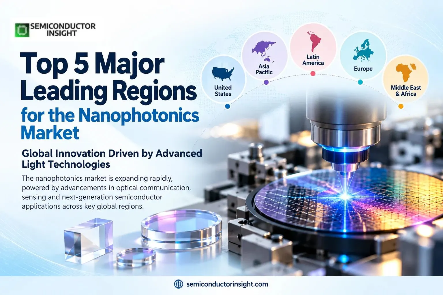
Top 5 Major Leading Regions for the Nanophotonics Market and the Race to Build AI-Ready Optical Chips, Quantum Devices and Nanoscale Light Systems
Nanophotonics studies how light behaves and can be controlled at dimensions close to or below its wavelength. By engineering nanostructures, researchers can manipulate light in compact devices for sensing, imaging, optical communication and computing. The field includes metasurfaces, plasmonic structures, quantum emitters and photonic integrated circuits, bringing optical functions into increasingly small footprints.
- The commercial significance is growing as AI systems require faster communication between processors, memory and networking equipment.
- A 2025 article in npj Nanophotonics examined optical switching and optical input/output approaches designed to reduce communication energy and latency.
- It discussed optical circuit switches with more than 64 to 128 ports and modulators operating above 100 GHz as technology targets under development, rather than specifications shared by every commercial product.
North America – Connecting AI Research with Photonic Manufacturing
The United States combines advanced computing research with photonic-device development, while Canada is strengthening manufacturing capability. In May 2026, the Government of Canada announced plans to spin off the National Research Council’s Canadian Photonics Fabrication Centre into a commercial entity.
The facility has supported compound-semiconductor and photonic-device development for approximately two decades. This move is intended to expand domestic manufacturing capacity and support applications in AI, aerospace, defence and advanced manufacturing.
Europe – Turning Public Research into Integrated Photonic Chips
Europe has established photonics research networks and companies working on optical components, integrated devices and manufacturing processes. The UK’s 2026 semiconductor sector study estimated that public semiconductor-related research and innovation funding reached £1.8 billion by the end of 2025.
Among new allocations during 2024 and 2025, photonic integrated circuit design and fabrication accounted for approximately 11%. This demonstrates institutional investment in photonic-chip capabilities, although it is not a nanophotonics market-share figure.
Asia Pacific – Scaling Optical Components and Semiconductor Expertise
Asia Pacific has a broad photonics manufacturing base, particularly across China, Japan, South Korea and Taiwan. A 2026 SPIE industry report noted that 56% of 5,417 photonics companies tracked for 2024 were headquartered in Asia, compared with 22% in Europe and 21% in North America.
- The figures cover the wider photonics industry, not nanophotonics alone, but help illustrate the region’s extensive supplier ecosystem.
Latin America – Building Specialised Photonics Networks
Latin America’s opportunities centre on research-led development, optical instrumentation, sensing and specialised component design. Mexico has an organised photonics cluster listed by the IEEE Photonics Society, providing an industry network through which researchers and businesses can connect.
Wider adoption will depend on access to fabrication facilities, skilled engineers and partnerships that help convert laboratory prototypes into manufacturable products.
You Can Go Through Our Latest Updated Insights Here: https://semiconductorinsight.com/report/nanophotonics-market/
Middle East & Africa – Developing Research Niches and Applications
The Middle East and Africa have emerging photonics networks and research activity in areas including optical communications, sensing and quantum technologies. The IEEE Photonics Society lists organisations and clusters such as Photonics Ghana and Photonics Israel.
These networks provide a foundation for collaboration, although their presence alone does not establish regional market dominance. Nanophotonic sensors and optical components may find specialised uses in environmental monitoring, medical diagnostics and communications infrastructure.
India’s Photonic Chip Work Reaches a New Milestone
India is also developing its own photonic-chip design and testing capabilities. In April 2026, the Ministry of Electronics and Information Technology announced a silicon photonics process design kit and a universal test engine for programmable photonic integrated circuits developed through IIT Madras’s CoE-CPPICS. Shared design and test infrastructure can help researchers validate devices more efficiently and reduce barriers to experimentation.
AI Infrastructure Is Bringing Photonics Closer to the Processor
- As computing systems scale, moving data between chips can become as important as processing it.
- Nanophotonic components can guide, modulate or detect light in tightly integrated systems, potentially helping high-bandwidth links operate with lower energy overhead.
- However, practical deployment still depends on manufacturing yield, packaging, thermal control and integration with electronic circuits.
- In the United States, the National Institute of Standards and Technology conducts research into integrated nonlinear photonics, microresonator frequency combs and photonic circuits for communications, precision timing and advanced microelectronics.
- These programmes show how nanophotonics connects fundamental research with potential applications in computing and measurement.
What Will Determine Commercial Readiness?
The next stage for nanophotonics depends on repeatable fabrication, low-loss optical connections, reliable packaging and measurable advantages over conventional approaches. AI connectivity is creating a visible application pathway, while quantum devices, compact sensors and flat optical elements broaden the field’s potential reach. The key commercial question is whether promising nanoscale effects can be turned into robust components that manufacturers can produce, test and integrate at scale.

Comments (0)