

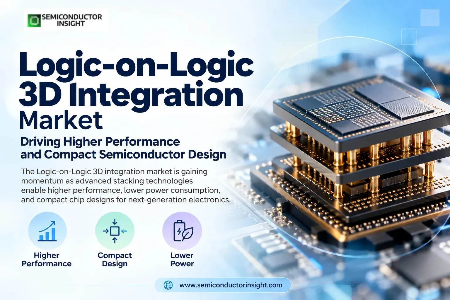
Top 5 Major Leading Regions for the Logic-on-Logic 3D Integration Market as High-Performance Computing Moves toward Vertical Architectures
Logic-on-logic 3D integration is changing how semiconductor designers approach computing performance. Instead of placing all processing functions on a single flat silicon die, manufacturers can stack two or more logic dies vertically and connect them using extremely dense interconnects.
This architecture can shorten signal paths, reduce communication delays and improve computing density, although thermal management, manufacturing yield and test complexity remain important engineering considerations.
The commercial backdrop is significant. The Semiconductor Industry Association reported that global semiconductor sales reached $791.7 billion in 2025, up 25.6% from 2024. AI processors, high-performance computing and increasingly sophisticated electronic systems are creating a stronger need to integrate computing functions efficiently.
Asia Pacific Turns Chip Stacking Into Manufacturing Reality
Asia Pacific holds the strongest manufacturing position because Taiwan, South Korea, Japan and other regional semiconductor hubs combine advanced fabrication, packaging, testing and electronics supply chains. Taiwan is particularly important through TSMC’s System on Integrated Chips (SoIC) technology, which supports wafer-level 3D integration and high-density connections between dies.
- TSMC reported that its 3-nanometre SoIC stacking technology entered volume production in 2025.
- In March 2026, Taiwan-based ASE also announced a NT$17.8 billion investment in two new buildings for advanced packaging and testing, expected to create approximately 1,470 jobs by completion in 2028.
These developments show how logic stacking is progressing from process research toward manufacturing infrastructure for AI, high-performance computing and high-speed communications.
Japan Strengthens the Materials and Process Engineering behind Stacking
Japan remains strategically relevant because advanced 3D integration depends on more than chip design. Silicon wafers, bonding materials, deposition processes, precision equipment and inspection systems all influence manufacturing yield. Japan’s Ministry of Economy, Trade and Industry selected Rapidus for next-generation semiconductor support in November 2025, with ¥100 billion allocated in the fiscal 2025 initial budget.
Although this initiative is not exclusively a logic-stacking programme, it strengthens Japan’s role in advanced semiconductor manufacturing. Its materials and equipment suppliers can support the process control required to align and bond increasingly complex chip structures.
North America Builds around AI Accelerators and Dense Compute
North America is a major innovation centre for advanced processor design, AI accelerators and data-centre hardware. Intel’s Foveros Direct technology uses copper-to-copper hybrid bonding to stack chiplets with interconnect pitches below 5 micrometres, supporting high-density connections for client and data-centre applications.
The region’s opportunity extends from chip architecture and design software to specialised packaging equipment and testing. For designers, logic-on-logic integration can enable different processing blocks to be combined without forcing every function onto the same manufacturing node. This matters when AI workloads demand greater parallel processing while keeping power consumption and latency under control.
Europe Connects Advanced Packaging with Industrial Chip Design
Europe’s strengths include semiconductor equipment, automotive electronics, and research institutions and specialised chip design. The European Chips Act aims to mobilise more than €43 billion in public investment and strengthen the region’s semiconductor ecosystem, with a target of reaching 20% of global semiconductor production by 2030.
For logic-on-logic integration, European opportunities include automotive processors, industrial control systems, communications hardware and specialised computing. The region’s established equipment and research networks can contribute to bonding precision, thermal analysis, inspection and reliability testing, even where the highest-volume stacking operations take place elsewhere.
Take a Quick Glance at Our In-Depth Analysis Report: https://semiconductorinsight.com/report/logic-on-logic-3d-integration-market/
Latin America and the Middle East Develop Supporting Roles
Latin America has a smaller footprint in leading-edge logic stacking, but its electronics manufacturing, automotive supply chains and engineering services can support downstream semiconductor applications. Mexico’s proximity to North American electronics production offers a particularly useful connection to computing hardware and industrial systems.
In the Middle East and Africa, the nearer-term opportunity lies in data-centre infrastructure, semiconductor research partnerships and specialised electronics deployment. These regions are not currently comparable with Taiwan or South Korea in high-volume logic-on-logic manufacturing, but growing demand for AI computing can strengthen their role as customers and ecosystem partners.
How the Technology Moves From Design to Deployment?
Logic-die design → Precision alignment → Hybrid bonding → Thermal and electrical validation → Package integration → System-level testing
The central development in 2026 is the transition from simply shrinking transistors to engineering the connections between separate computing dies. Asia Pacific currently has the strongest manufacturing ecosystem, North America contributes processor innovation, and Europe and Japan bring important equipment, research and materials capabilities. As AI computing expands into data centres, industrial systems and selected wearable devices, the ability to stack logic efficiently will become an increasingly important part of semiconductor design.

Comments (0)