

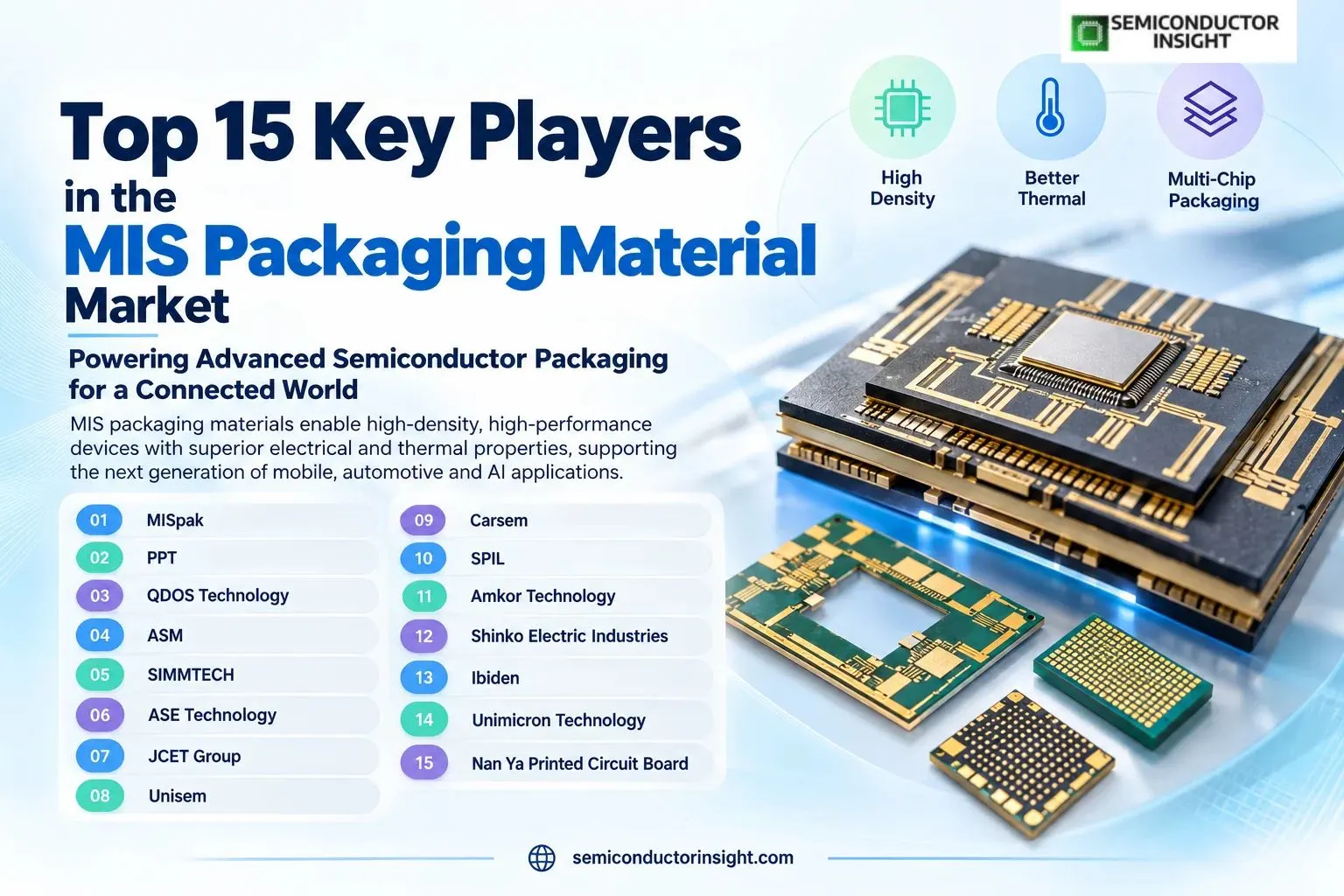
Top 15 Key Players in the MIS Packaging Material Industry Powering High-Performance Packaging Applications Worldwide
Molded Interconnect Substrate packaging materials redefine semiconductor integration by embedding copper traces within pre-molded structures, enabling finer line-and-space routing, robust flip-chip assembly, copper-filled vias for high-frequency performance, and improved thermal dissipation in compact packages.
These substrates support single- to multi-layer configurations that combine the density advantages of organic substrates with the thermal and process benefits of advanced leadframes. Applications span power management ICs, analog chips, RF and 5G modules, optical image stabilization units, fingerprint sensors, automotive electronics, LED drivers, and emerging server, data-center, and AIoT devices.
Demand continues to expand in 2026 as device makers pursue higher I/O counts, thinner profiles, and multi-chip modules for electric-vehicle control systems and high-performance computing.
MISpak advances MIS packaging materials through specialized single- and dual-layer substrates that deliver high routing density and multi-row QFN, BGA, MCM, SiP, and 3D configurations. The company’s solutions address power-management, touch-panel, wearable, and wireless-charging devices by integrating superior electrical and thermal characteristics. In recent production cycles, cumulative shipments of individual units have reached multi-billion levels, supporting dozens of customers across high-density packaging lines. Industry recognition includes contributions to semiconductor technology standards, while ongoing process refinements in 2026 focus on multi-functional component integration for next-generation mobile and power applications.
PPT supplies an extended range of MIS substrates spanning one-layer through six-layer constructions, enabling flexible design options for multi-chip packaging that traditional leadframe approaches struggle to match. These materials serve power and PMIC circuits, automotive electronics, RF and 5G modules, optical image stabilization, fingerprint recognition, third-generation semiconductors, and LED applications. Multi-layer windable leadframe variants further expand capability for complex assemblies. Current development activity centers on higher-layer counts and improved thermal paths to meet rising requirements from network communication and electric-vehicle control systems.
QDOS Technology produces one- to three-layer MIS substrates alongside related IC substrate and flexible circuit solutions using advanced semi-additive processes and ABF materials. Facilities across Malaysian and Chinese sites support coreless thin structures with any-shape copper vias that enhance thermal conductivity and enable package size reductions relative to conventional leadframes. Applications include mid-I/O thermal-critical devices, embedded antenna designs, power-management ICs based on gallium nitride, and high-reliability automotive and industrial modules. In 2026 the company continues to expand MIS ABF substrate offerings for wire-bond and flip-chip platforms while maintaining production capacity measured in tens of thousands of square meters monthly across multiple plants.
ASM develops and supplies molded interconnect packaging materials under its Buildup Interconnect Technology platform, supporting advanced package assembly for thinner consumer and wearable devices. Collaboration efforts have included joint entities focused on multi-layer redistribution-layer carriers that accommodate wire-bond, flip-chip, and multi-chip configurations. These materials address system-in-package and IoT requirements with fine routable traces and copper pads. Recent 2026 activity emphasizes advanced packaging tool demand driven by AI infrastructure, with strong order momentum for thermo-compression bonding and related substrate-compatible solutions that integrate MIS-style interconnects.
SIMMTECH delivers high-density semiconductor package substrates that complement MIS approaches through fine-pitch patterning, thin constructions, and thermal-management features suited to automotive and mobile devices. Product lines include wire-bond and flip-chip chip-scale packages, slim FCBGA variants, and module boards for AI server memory. At industry exhibitions in 2026 the company highlighted SOCAMM module PCBs and LPDDR package substrates for high-bandwidth memory applications, along with ultra-thin and fine-pitch technologies that improve heat dissipation under rising power densities. Additional developments cover rigid-flex structures and exploratory glass-substrate research aimed at reducing warpage in large-area packages.
ASE Technology integrates MIS-compatible packaging flows within its advanced assembly portfolio, enabling high-density interconnects for analog, power, and RF devices. The company processes large volumes of packages that leverage pre-molded substrate advantages for fine-pitch and multi-die configurations. Ongoing 2026 programs focus on system-in-package and fan-out platforms that benefit from the thermal and electrical performance of molded interconnect structures, supporting customer transitions toward smaller form factors in mobile and automotive electronics.
JCET Group applies MIS substrate technology in selected power and analog packaging lines, capitalizing on the embedded copper-trace architecture for improved thermal paths and higher I/O density. Production supports multi-chip modules and leaded package alternatives that meet reliability demands in industrial and consumer applications. Current capacity utilization reflects growing adoption of these materials for devices requiring robust flip-chip assembly and high-frequency performance.
To Stay Tuned with More meaningful and In-Depth Insights, Do Visit here: https://semiconductorinsight.com/report/global-mis-packaging-material-market/
Unisem incorporates molded interconnect substrates into its assembly processes for RF, power, and sensor packages, delivering low-profile solutions with fine routing. The technology enables multi-die and system-in-package constructions that address space constraints in wireless and automotive modules. 2026 developments emphasize higher-volume qualification of MIS-based platforms for emerging 5G and AIoT components.
Carsem utilizes MIS packaging materials to achieve denser interconnects and better heat dissipation in power IC and analog devices. Assembly lines process substrates that support both wire-bond and flip-chip methods within compact footprints. Recent process optimizations target increased throughput for multi-row and multi-chip configurations demanded by electric-vehicle and industrial control markets.
SPIL collaborates on molded interconnect substrate manufacturing and assembly, focusing on redistribution-layer carriers suited to advanced packages. Joint initiatives have advanced multi-layer MIS capability for system-in-package and IoT applications. In the current environment the emphasis remains on fine-trace performance and copper-pad reliability for high-density consumer and communication devices.
Amkor Technology deploys MIS-compatible substrates across selected power, RF, and analog packaging platforms, benefiting from the thermal advantages of copper-filled vias. High-volume production lines handle packages that require thinner profiles and elevated I/O counts. 2026 programs continue to expand advanced packaging options that integrate these materials for automotive and high-performance computing modules.
Shinko Electric Industries develops substrate technologies that align with MIS principles for fine-line routing and thermal management in power and high-frequency packages. Production supports multi-layer constructions used in automotive electronics and RF modules. Ongoing refinements address the demand for higher-density interconnects in next-generation semiconductor packages.
Ibiden supplies advanced packaging substrates that complement MIS approaches through high-density patterning and thermal performance features. These materials serve applications in power management, RF, and multi-chip modules. Current capacity supports the transition toward finer geometries required by 5G infrastructure and electric-vehicle control systems.
Unimicron Technology produces high-density interconnect substrates applicable to MIS-style packaging for analog, power, and sensor devices. Fine-pitch capabilities enable compact multi-die assemblies with improved electrical characteristics. 2026 efforts focus on materials that enhance signal integrity and heat dissipation for high-frequency and high-power applications.
Nan Ya Printed Circuit Board contributes specialized substrate solutions that support the density and thermal requirements of molded interconnect packaging. Production lines deliver materials suited to RF, power IC, and automotive electronics. Recent process advancements target multi-layer configurations that meet the evolving needs of data-center and AIoT packaging platforms.

Comments (0)