

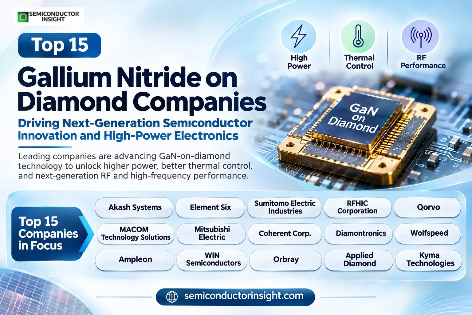
Top 15 Gallium Nitride on Diamond Companies Driving Next-Generation Semiconductor Innovation and High-Power Electronics
Gallium Nitride on Diamond market sits at the intersection of high-frequency semiconductor engineering and advanced thermal materials. It combines GaN’s ability to operate at high power and high frequencies with diamond’s exceptional ability to conduct heat away from a device.
The objective is not simply to make a faster transistor; it is to control the heat generated in increasingly compact RF components so that they can sustain demanding operating conditions.
Akash Systems – Turning GaN-on-Diamond Engineering Into a Commercial Product Platform
Akash Systems stands out because its work connects GaN-on-diamond technology with practical high-performance communication hardware. Its approach uses synthetic diamond to extract heat from GaN devices, addressing a major limitation in high-power RF electronics. The company is particularly relevant to satellite communications, where compact equipment, thermal stability and power efficiency directly influence payload capability.
Its satellite radio specifications illustrate this focus on system-level performance. Akash lists a 700 Mbps downlink, extendable to 1.4 Gbps, within a compact 10 cm × 10 cm × 3 cm form factor. The product is also specified for DC power consumption below 28 W. In February 2026, the company announced delivery of diamond-cooled NVIDIA H200 GPU servers to India’s NxtGen AI, extending its diamond-cooling approach into data-centre infrastructure. Its March 2026 announcement of diamond-cooled AMD Instinct MI350X servers further demonstrated an expansion beyond satellite radio applications. These deployments make Akash one of the most commercially visible names associated with diamond-based thermal solutions.
Element Six – Engineering Diamond Materials for High-Power RF Devices
Element Six occupies a strategically important position because the performance of a GaN-on-diamond device depends heavily on the quality of its diamond layer. Its CVD diamond portfolio is designed for heat spreading in RF power amplifiers, AI accelerators, GPUs and other semiconductor applications. Rather than competing only at the transistor level, the company addresses the material interface where heat must leave the active device efficiently.
Its technical specifications provide a useful indication of the opportunity. Element Six offers CVD diamond with thermal conductivity ranging from 1,000 to 2,200 W/m·K, depending on the material grade. Its published RF case studies report a 30% reduction in thermal resistance when diamond heat spreaders are used in an RF package. The company also highlights diamond-based RF resistors operating above 20 GHz. Its collaboration with Orbray on single-crystal synthetic diamond wafers adds another important dimension: moving from individual heat spreaders towards wafer-level integration. This positions Element Six as a central materials supplier for next-generation thermal architectures.
Sumitomo Electric Industries – Connecting Diamond Composite Engineering With Power Electronics
Sumitomo Electric Industries brings an important materials-engineering perspective to the GaN-on-diamond ecosystem. Its relevance comes from high-performance heat-spreading substrates, including silver-diamond and other composite materials used in demanding power semiconductor environments. These materials are designed to manage heat while addressing mechanical compatibility with semiconductor packages.
The company’s 2025 corporate profile identifies silver-diamond, copper-molybdenum and copper-tungsten heat-dissipation substrates as products supporting power semiconductors used in electric vehicles, aerospace, wireless communications and optical communications. This matters because a thermal solution must do more than offer high conductivity: it must also account for thermal expansion, mechanical stress and packaging reliability. Sumitomo’s experience with multiple composite systems gives it a useful position in applications where diamond-based materials may be integrated into larger power modules. Its role should be understood as an adjacent thermal-materials capability rather than evidence of a commercially established GaN-on-diamond transistor portfolio.
RFHIC Corporation – Bringing GaN Device Experience Into the Diamond Materials Segment
RFHIC is particularly significant because it combines established GaN RF engineering with a direct move into CVD diamond heat spreaders. Its traditional strength lies in GaN-on-SiC transistors and RF systems used in wireless infrastructure, radar, aerospace and industrial RF energy applications. These are precisely the environments where heat removal becomes a major design consideration.
In September 2026, RFHIC announced its DiaFlux family of thermal-grade polycrystalline CVD diamond heat spreaders. The initial range includes DiaFlux 150, specified at 1,500 W/m·K, and DiaFlux 180, specified at 1,800 W/m·K at 25°C. The company describes applications spanning chips, plates, heat spreaders and wafer formats, with electrically insulating material options. The significance is strategic: RFHIC is extending its understanding of heat generation inside high-power GaN devices into the material used to manage that heat. This combination of device knowledge and diamond-material development makes it one of the most directly relevant participants in the evolving ecosystem.
Qorvo – Demonstrating the RF Performance Requirements That Diamond Integration Must Address
Qorvo is an important reference point for the performance requirements driving interest in GaN-on-diamond. Its commercial GaN portfolio is primarily based on GaN-on-SiC, not GaN-on-diamond, but its products demonstrate the high-frequency and high-power operating conditions where improved thermal management could become valuable.
One example is the QPA2811 X-band amplifier, which covers 8.5-10.55 GHz and delivers 60 W saturated output power. The device uses Qorvo’s 0.15 μm GaN-on-SiC process and is packaged in a 7 mm × 7 mm, 48-pin format. Another example, the QPA2212, operates across 27.5-31 GHz with 20 W saturated output power for satellite communications and 5G infrastructure. These specifications show why heat extraction is important as RF devices become more compact and operate at demanding power levels. Qorvo’s relevance is therefore strongest as a major GaN device developer and potential application-side beneficiary of advanced diamond thermal integration.
MACOM Technology Solutions – Strengthening the RF Manufacturing Base for Advanced GaN Devices
MACOM’s importance comes from its combination of RF semiconductor products, foundry services and GaN manufacturing capability. This gives the company a position beyond component sales: it can support customers developing custom GaN monolithic microwave integrated circuits for communications and defence applications.
A major development took place in July 2025, when MACOM completed the transfer of the Research Triangle Park wafer fabrication facility. The facility includes a 100 mm GaN production line and manufactures GaN-on-SiC process technologies for RF power devices and MMICs. It is also a US Department of Defense Trusted Foundry. This manufacturing capability is relevant to the GaN-on-diamond ecosystem because advanced thermal materials must ultimately integrate with repeatable semiconductor fabrication and packaging processes. MACOM is not being presented here as a current commercial GaN-on-diamond supplier; its strategic importance lies in its RF device manufacturing infrastructure and the potential for future thermal-material integration.
Don’t Forget to Surf Our Updated Report for More Detailed Analysis: https://semiconductorinsight.com/report/gallium-nitride-on-diamond-market/
Mitsubishi Electric – Advancing Higher-Frequency GaN Power Amplification for 5G-Advanced
Mitsubishi Electric is relevant because its RF development programme is moving into frequency ranges where thermal management, compact packaging and power efficiency become increasingly demanding. Its GaN power amplifier work supports the evolution of 5G-Advanced infrastructure and provides a potential application pathway for advanced heat-spreading materials.
In June 2025, the company announced performance verification of a 7 GHz GaN power amplifier module for 5G-Advanced base stations. The development is significant because higher-frequency base-station architectures require power amplifiers that can deliver strong output while remaining compact and efficient. As network operators prepare for more advanced radio configurations, device temperature and long-term reliability become important design considerations. Mitsubishi Electric’s relevance to GaN-on-diamond is therefore tied to the demanding operating conditions of its GaN RF platforms. Its public announcement demonstrates GaN module development, not a confirmed commercial transition to diamond substrates.
Coherent Corp. – Making Diamond-to-Semiconductor Bonding More Practical
Coherent has strengthened its position in diamond-enabled semiconductor thermal management through its work on bondable diamond solutions. Its January 19, 2026 announcement introduced a diamond material with specialised surface preparation designed to support direct bonding to semiconductor dies. This is an important development because thermal resistance at the interface between a chip and its heat spreader can limit the benefits of using a highly conductive material.
The company’s solution is engineered with controlled surface roughness, flatness, coatings and preparation. It is designed for compatibility with several semiconductor materials, including GaN, aluminium gallium nitride, silicon, silicon carbide, gallium arsenide and indium phosphide. This multi-material approach broadens its relevance beyond one device category. For GaN-on-diamond development, the ability to create a reliable bond between the active semiconductor and the diamond layer is a key manufacturing consideration. Coherent’s 2026 launch makes it a particularly important company to monitor as diamond integration moves towards more manufacturable packaging formats.
Diamontronics – Moving Chip-Level Diamond Cooling Towards Wafer-Scale Validation
Diamontronics represents an emerging technology-development participant focused on diamond-based thermal management for advanced semiconductors. Its work is centred on diamond bonding wafers and chip-level thermal solutions rather than established high-volume RF transistor production. The company’s relevance is particularly strong as semiconductor designers look for ways to manage localised heat in increasingly dense chips.
Its 2026 milestone is notable: Diamontronics announced completion of a proof-of-concept financing round intended to accelerate process validation for chip-level diamond thermal solutions and atomic-scale ultra-precision polishing equipment. The company’s development pathway is important because surface quality and bonding precision influence thermal contact resistance and manufacturing yield. Its stated application interests include high-performance computing, AI chips and wireless communications. While it remains an emerging player rather than a proven large-scale supplier, its focus on wafer-level process validation makes it relevant to the next generation of diamond-integrated semiconductor packaging.
Wolfspeed – Providing a Wide-Bandgap Benchmark for Thermal and RF Device Design
Wolfspeed’s position in this landscape requires an important distinction. The company is primarily focused on silicon carbide semiconductor technology and should not be described as a current leading GaN-on-diamond manufacturer. Its relevance comes from its historical RF GaN activities and its wider role in the development of wide-bandgap semiconductor technology.
In December 2023, Wolfspeed completed the sale of its RF business to MACOM. The transaction transferred the RF business, while Wolfspeed continued its transformation towards a pure-play silicon carbide semiconductor manufacturer. This distinction matters when assessing the current competitive landscape: MACOM now carries the direct operating relevance of the acquired RF business, while Wolfspeed remains important as a SiC technology benchmark. For GaN-on-diamond, the comparison is technically useful because designers evaluate different wide-bandgap platforms according to power density, thermal resistance, operating frequency and device reliability. Wolfspeed therefore belongs in an adjacent technology comparison, not among confirmed commercial GaN-on-diamond suppliers.
Ampleon – Expanding High-Power GaN RF Designs for Demanding Infrastructure
Ampleon is an additional relevant participant because its GaN RF portfolio addresses high-power applications where heat management is central to system performance. The company serves wireless infrastructure and industrial RF markets, with products designed for demanding power levels and operating conditions. Although its published GaN products are based on GaN-on-SiC, they illustrate the device requirements that can create demand for improved diamond heat-spreading technologies.
Its 2026 product announcements show the breadth of its RF activity. In August, Ampleon introduced an 800 W GaN-on-SiC HEMT for the 902-928 MHz ISM band. In June, it announced a 1.6 kW-class GaN-SiC transistor for 600 MHz industrial and accelerator applications. The company also introduced a fully integrated 5G massive-MIMO GaN power amplifier module in June 2026. These developments demonstrate the continuing push towards higher-output RF systems. Ampleon’s importance to the GaN-on-diamond market is therefore as a high-power GaN device specialist whose future product architectures could benefit from more effective thermal interfaces.
WIN Semiconductors – Creating a Foundry Route for Higher-Power GaN MMIC Designs
WIN Semiconductors adds an important manufacturing dimension to the GaN-on-diamond ecosystem. As a compound-semiconductor foundry, it supports customers that design RF and microwave integrated circuits but rely on specialised fabrication processes to manufacture them. This role becomes increasingly important as GaN devices move into more complex front-end architectures.
In June 2026, WIN announced qualification of its NP12-0B GaN process for 40 V operation. The platform uses a 0.12 μm gate-length GaN-on-SiC process and supports power amplifiers, transmit/receive switches and single-chip front-end MMICs. The development is relevant to 5G, satellite communications and radar applications. WIN also worked with Keysight on a GaN MMIC design workflow announced in June 2026, integrating simulation, 3D layout verification and evaluation-board design. These developments do not establish a GaN-on-diamond product, but they show how foundry readiness and design verification can support future integration of advanced thermal materials into RF semiconductor production.
Orbray – Developing Precision Diamond Wafers for Semiconductor Integration
Orbray’s contribution is centred on the difficult manufacturing steps required to turn synthetic diamond into a usable semiconductor substrate or heat-spreading platform. Diamond’s hardness and thermal properties make it attractive for advanced electronics, but producing large, flat and highly polished wafers is a demanding engineering task. Orbray has developed specialised polishing techniques to address this requirement.
The company received the Semiconductor of the Year award in 2022 for its industrial production technology for 2-inch diamond wafers. It subsequently entered a strategic partnership with Element Six in June 2024 to develop larger-diameter single-crystal diamond substrates. This collaboration is significant because wafer dimensions, surface flatness and bonding quality all affect whether diamond can be integrated into semiconductor manufacturing at scale. Orbray’s work is particularly relevant to future wafer-level thermal management and diamond-based semiconductor structures. Its role is best understood as a specialist in diamond wafer processing and substrate engineering.
Applied Diamond – Supplying Engineered CVD Heat Spreaders for High-Power Electronics
Applied Diamond is relevant to GaN-on-diamond through its CVD diamond growth, finishing and heat-spreader capabilities. The company supplies diamond thermal components for electronic devices, power transistors, radar arrays, amplifiers and laser systems. These are applications where heat concentration can constrain device output and reliability.
Its published heat-spreader portfolio provides three thermal grades: black diamond at approximately 700-800 W/m·K, opaque diamond at 900-1,000 W/m·K and optically clear diamond at 1,700-1,800 W/m·K. The company also describes heat spreaders grown on 2-inch wafers, which can be laser-cut into customer-specific sizes. Available thicknesses extend up to 1 mm, with options for patterned metallisation and electrical isolation. These specifications are relevant because GaN-on-diamond integration requires more than a high-conductivity material: the diamond must also be finished, shaped and metallised to suit the semiconductor die and package. Applied Diamond’s position is strongest in engineered thermal components and custom material processing.
Kyma Technologies – Supporting the GaN Epitaxy and Device Development Side
Kyma Technologies is an additional ecosystem participant because GaN-on-diamond development depends on high-quality GaN material and device structures before diamond integration can be considered. The company works on compound-semiconductor materials and processes, including GaN-related technologies for high-performance electronic devices.
A relevant example is its 2024 US Department of Defense Phase II SBIR award for pulsed sputter deposition technology aimed at GaN HEMT contacts. The award was approximately US$1.2 million and involved work with the US Navy. The project sought to develop a lower-cost contact process for GaN HEMT epiwafers, with the stated aim of reducing process cost by a factor of three compared with the existing approach. GaN HEMTs are used in radar, satellite communications, GPS, surveillance and wireless infrastructure. Kyma’s contribution is therefore upstream: improving GaN device processing and epitaxial technology that could support future high-performance platforms. It should be regarded as an adjacent GaN technology developer, not a confirmed producer of commercial GaN-on-diamond wafers.

Comments (0)