
Top 5 Dominant Geographic Markets Influencing the Future of the Strain Gage Industry
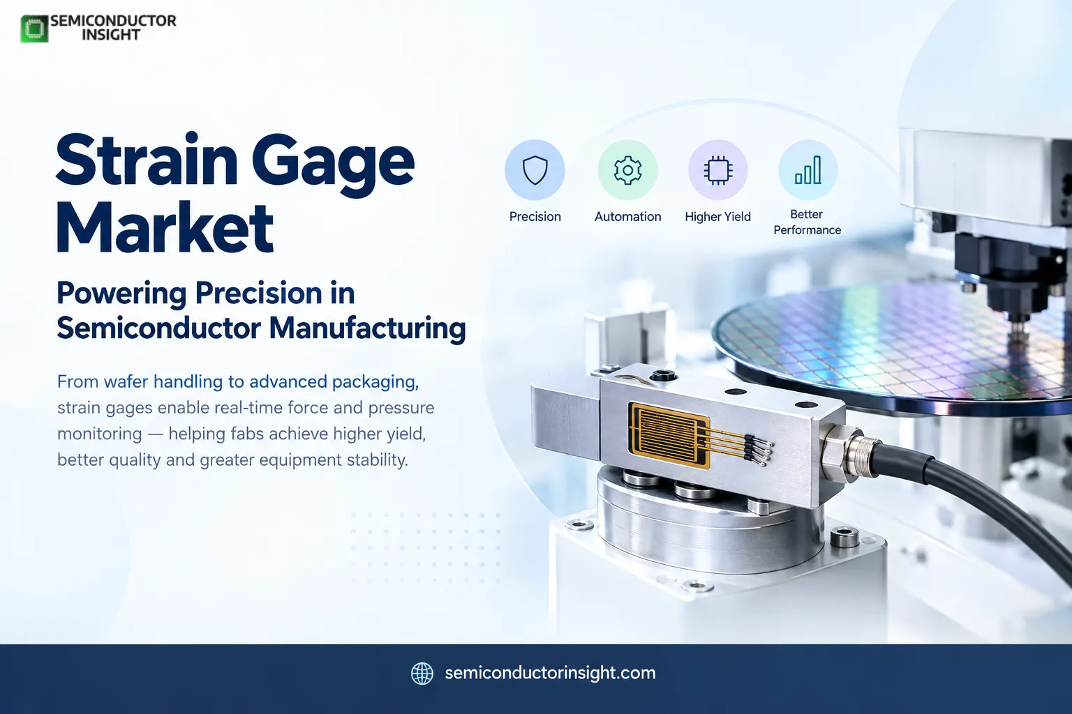
Strain Gage Market is finding an increasingly important role inside semiconductor manufacturing, where tiny variations in force can affect wafer integrity, bonding quality, equipment stability and final package performance.
Modern strain gages convert mechanical deformation into electrical signals, making them useful in load cells, force transducers and precision measurement systems. Semiconductor manufacturing applications now extend across wafer handling, die bonding, wire bonding, dicing, polishing, inspection and testing.
Why strain measurement is becoming a process-control issue?
Semiconductor production is moving toward increasingly automated and tightly controlled processes. Equipment builders need to know not simply whether a machine is operating, but whether the correct mechanical force is being applied at the right moment.
This is particularly relevant during die attach. FUTEK notes that semiconductor dies require controlled force during processes such as TSV, eutectic, epoxy and solder-based attachment, because excessive or inconsistent force can damage chips or produce incomplete bonds. Load cells using strain-gage technology can provide closed-loop control for these operations.
From wafer movement to advanced packaging
The application landscape is expanding beyond traditional force measurement. Semiconductor equipment can use sensing systems during wafer handling, grinding, dicing, CMP, die sorting, wire bonding, flip-chip assembly and encapsulation. These processes increasingly require real-time monitoring of mechanical stress, pressure and vibration.
Fujifilm also identifies wafer-bonding equipment as an application where force measurement is used to evaluate contact conditions, while substrate stacking and lamination processes require controlled load measurement.
North America turns semiconductor investment into sensor demand
- North America remains an important technology and manufacturing hub for precision force measurement.
- The U.S. semiconductor build-out is creating new requirements for wafer fabrication, packaging and equipment validation.
- In June 2025, the U.S. Department of Commerce reported Micron’s planned $200 billion semiconductor manufacturing and R&D investment across Idaho, New York and Virginia, with the projects expected to create around 90,000 jobs.
- The region’s advanced packaging push is also significant. The U.S. Commerce Department finalized $1.4 billion in awards in January 2025 for the National Advanced Packaging Manufacturing Program.
Asia-Pacific remains the center of high-volume chip production
Asia-Pacific has the strongest connection between semiconductor manufacturing scale and precision sensing demand. Global semiconductor sales reached $791.7 billion in 2025, while Asia Pacific and other markets recorded 45% annual sales growth.
Japan is also rebuilding advanced semiconductor capacity. By February 2026, government and private companies had invested ¥267.6 billion in Rapidus, including participation from 32 companies. These investments support a wider equipment ecosystem where compact force and strain measurement can be incorporated into automated manufacturing tools.
Europe is building a more localized semiconductor equipment ecosystem
Europe is strengthening semiconductor manufacturing, packaging and pilot-line capabilities, creating another application base for precision sensing. The European Commission says the Chips Act has mobilized more than €52 billion in public and private investment and estimates around 46,000 direct and indirect jobs.
In February 2026, Europe launched the NanoIC pilot line at imec Leuven with total investment of €2.5 billion. The facility supports chip technologies below 2 nm and allows companies to test chip designs, equipment and processes at near-industrial scale.
To find out more, feel free to browse our latest updated report: https://semiconductorinsight.com/report/strain-gage-market/
Latin America is strengthening its domestic semiconductor capabilities
- Latin America’s opportunity is increasingly linked to electronics manufacturing, semiconductor design and localized production rather than only high-volume wafer fabrication.
- Brazil’s Brasil Semicon program was established to strengthen the complete semiconductor chain, including chip design, research, production and innovation.
- In June 2026, Brazil’s BNDES approved R$143.3 million for Zilia Technologies to expand semiconductor production and R&D in São Paulo.
- The components produced support smartphones, computers, automobiles, printers and security equipment.
Middle East & Africa build demand through industrial automation
The Middle East & Africa opportunity is emerging through industrial automation, electronics assembly, advanced manufacturing and technology diversification. Semiconductor-related investments can increase demand for precision sensing across automated machinery, testing systems and equipment maintenance.
The importance of this sensor category extends beyond semiconductor fabs themselves. Strain-gage load cells can provide force inputs for robotic handling, vibration monitoring, fabrication, testing and packaging systems used in semiconductor facilities.
The next specification race is happening inside the equipment
Strain Gage Market is increasingly being shaped by equipment-level requirements rather than standalone sensor demand. Smaller packages, higher sensitivity, temperature compensation, faster response and integration with automated controls are becoming important selection criteria.
As semiconductor fabs add more robotics and advanced packaging processes, strain measurement is moving closer to the machine’s control architecture, making precision sensing an increasingly practical part of semiconductor manufacturing infrastructure.

Comments (0)