
Top 10 Wafer Fab Equipment Companies Powering the AI Chip Boom in 2026
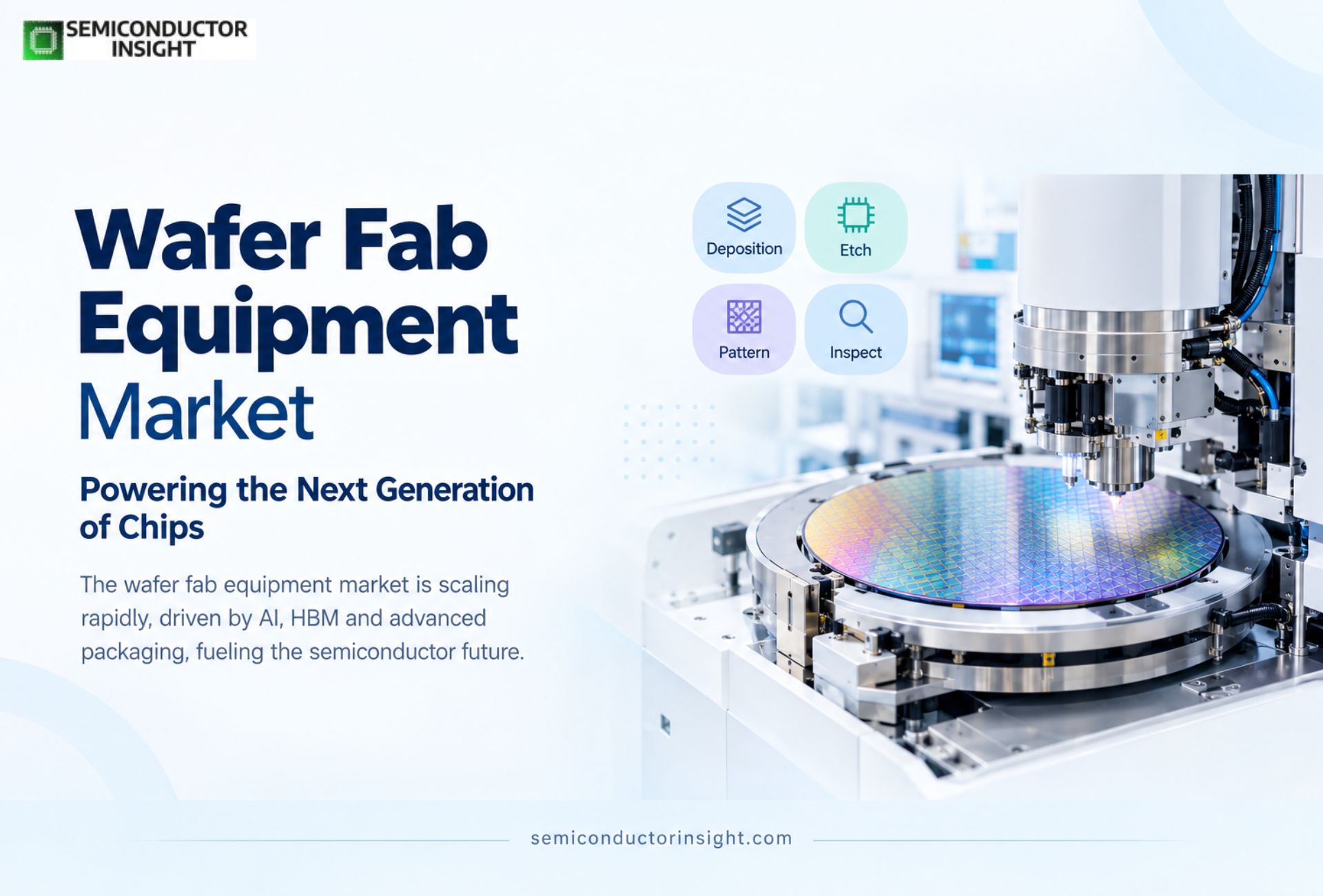
The wafer fab equipment (WFE) market is the invisible engine of the semiconductor industry. Without the machines that deposit, etch, pattern, and inspect silicon wafers, there are no AI accelerators, no high-bandwidth memory, no advanced smartphones. In 2026, that engine is running hotter than ever. SEMI, the industry trade association, projects global WFE sales to reach USD143.9 billion this year, a 23.1% increase from 2025, driven by surging investment in leading-edge logic, HBM-related DRAM, and advanced packaging. By 2034, the market is estimated to reach USD179,772 million, growing at a 6.8% compound annual rate. But the market is not evenly distributed. Five companies – ASML, Applied Materials, Lam Research, Tokyo Electron, and KLA – together account for roughly 70% of global WFE revenue. Here is a closer look at the ten players shaping the fab equipment landscape in 2026.
- ASML Holding (Netherlands)
ASML is the undisputed gatekeeper of the most advanced chipmaking on the planet. Its extreme ultraviolet (EUV) lithography systems are the only tools capable of patterning the critical layers of logic chips at 7nm and below. In 2026, ASML accounts for about a quarter of global WFE sales. The company shipped its first High-NA EUV systems to Intel and imec this year, enabling 8nm resolution and pushing the industry toward the 2nm gate-all-around era. Intel has already used High-NA EUV for volume production of its Panther Lake processors, a milestone that validates the technology’s readiness for mass manufacturing. ASML plans to increase Low-NA EUV capacity by 30% in 2027 to meet demand from TSMC, Samsung, and Intel.
- Applied Materials (United States)
Applied Materials has the broadest portfolio in the WFE industry, spanning deposition, etch, ion implantation, chemical mechanical planarization, and metrology. That breadth is a strategic advantage. Management expects leading-edge foundry-logic, DRAM, and advanced packaging to account for roughly 80% of WFE growth in 2026 and 2027. The company introduced six new chipmaking systems in its latest quarter, including tools targeting HBM packaging and 3D chiplet stacking. Applied Materials expects advanced packaging revenues to grow more than 70% in 2026, and its DRAM revenues, including HBM packaging, rose 52% year-over-year in the fiscal third quarter. It plans to double quarterly system output by 2028.
- Lam Research (United States)
Lam Research is the dominant force in etch and deposition, the process steps that are becoming more critical as chip architectures grow more complex. The company holds a 43% share of the conductor etch market, followed by Tokyo Electron at 20% and Applied Materials at 19%. AI workloads are driving significantly higher etch and deposition intensity, expanding Lam’s served available market to above the mid-30% range of WFE in 2026. The company secured multiple critical etch wins at a major DRAM manufacturer with its new Akara etch system, which supports 3D DRAM architectures. Lam raised its 2026 WFE outlook to the USD135 billion range and sees continued growth into 2027.
- Tokyo Electron (Japan)
Tokyo Electron (TEL) is Japan’s largest semiconductor equipment maker and a comprehensive supplier of etching, deposition, coating/developing, cleaning, and wafer probing systems. The company has a bullish view on the market, forecasting 15% growth in the WFE market for calendar year 2026, above the consensus estimate. TEL ships over 4,000 units annually and has an installed base exceeding 100,000 systems globally, generating a stable stream of service revenue. Its coating/developer systems are essential for EUV lithography, giving it a strategic position alongside ASML in the most advanced fabs.
- KLA Corporation (United States)
KLA dominates process control, wafer inspection, and yield management. In an era of extreme complexity, that dominance is becoming more valuable. KLA expects its semiconductor process control systems business to grow more than 20% in 2026, outpacing the broader WFE market, driven by rising process control intensity and growth in advanced packaging. The company raised its advanced packaging process control revenue outlook to roughly USD1.1 billion for calendar 2026, up from about USD635 million in 2025. As chip designs grow more complex and defects become harder to detect, KLA’s inspection and metrology tools become indispensable.
- ASM International (Netherlands)
ASM International is a specialist in atomic layer deposition (ALD) and other thin-film deposition technologies. ALD is critical for depositing ultra-thin, highly uniform films in gate-all-around transistors, 3D NAND, and advanced DRAM. ASM has been a key beneficiary of the industry’s shift toward more materials-intensive manufacturing. Goldman Sachs named ASM International among its top WFE stock picks for 2026, alongside Applied Materials, Lam Research, ASML, and Tokyo Electron. The company’s focus on deposition technologies that enable higher-performance, lower-power chips positions it well for the AI-driven buildout.
- Screen Holdings (Japan)
Screen Holdings is a leading supplier of wafer cleaning equipment, a process step that occurs dozens of times during the fabrication of an advanced logic or memory chip. Cleaning is essential for removing particles, organic residues, and metallic contaminants that would otherwise kill device yield. As nodes shrink and defect tolerances tighten, the demand for advanced cleaning tools grows. Screen also supplies coating and developing systems that complement its cleaning portfolio. The company is a consistent performer in the Japanese semiconductor equipment sector and benefits from the global expansion of fab capacity in Japan, Korea, Taiwan, and the United States.
- Advantest (Japan)
Advantest is a leader in semiconductor test equipment, a segment that is growing rapidly as AI and HBM devices require more rigorous performance and reliability testing. SEMI projects semiconductor test equipment sales to increase 31.0% to USD15.3 billion in 2026, following a 55.3% surge in 2025. Advantest supplies test systems for logic, memory, and system-on-chip devices, and its tools are used extensively in the production of AI accelerators and high-bandwidth memory. The company’s strong position in the Japanese market and its growing international footprint make it a key player in the back-end equipment ecosystem that supports WFE.
- NAURA Technology (China)
NAURA Technology Group is China’s largest semiconductor equipment manufacturer, supplying etching, deposition, cleaning, and thermal processing tools. As China continues to invest heavily in domestic chip production, NAURA has emerged as a critical supplier for Chinese fabs seeking to reduce reliance on imported equipment. The company is particularly strong in deposition, etch, and CMP, though it remains negligible in lithography and metrology. Bernstein included NAURA among six leading semiconductor equipment companies in China and the United States to receive an Outperform rating, with a price target of CNY 680. NAURA’s growth reflects the broader trend of Chinese equipment vendors gaining share at the margins of a market still dominated by Western and Japanese incumbents.
- ACM Research (United States/China)
ACM Research specializes in wafer cleaning, plating, and advanced packaging equipment. The company has carved out a niche in single-wafer cleaning tools that are used in both front-end and back-end processes. As advanced packaging becomes more important for AI chips – particularly for HBM stacking and chiplet integration – ACM’s plating and cleaning tools are finding new applications. The company operates primarily in China but has been expanding its presence in other markets. It represents the kind of specialized, agile equipment supplier that is gaining traction as the WFE market fragments into more specialized segments.
What the Top Ten Reveal
The WFE market in 2026 is a study in concentration and fragmentation. The top five players control roughly 70% of revenue, a structure that reflects the enormous barriers to entry in lithography, deposition, and process control. But below that top tier, a diverse group of specialists – ASM International in ALD, Screen in cleaning, Advantest in test, NAURA in domestic Chinese supply – are finding growth in the niches that the giants cannot cover alone. The AI boom is pulling investment across the entire fab equipment ecosystem, from the EUV scanners that pattern the smallest features to the test systems that ensure every AI chip performs to specification. The 6.8% compound annual growth rate projected through 2034 will not lift all players equally, but it will lift the market as a whole. For the companies on this list, the challenge is not finding demand. It is keeping up with it.
Access All Data in the Detailed Report: https://semiconductorinsight.com/report/wafer-fab-equipment-wfe-market/

Comments (0)