
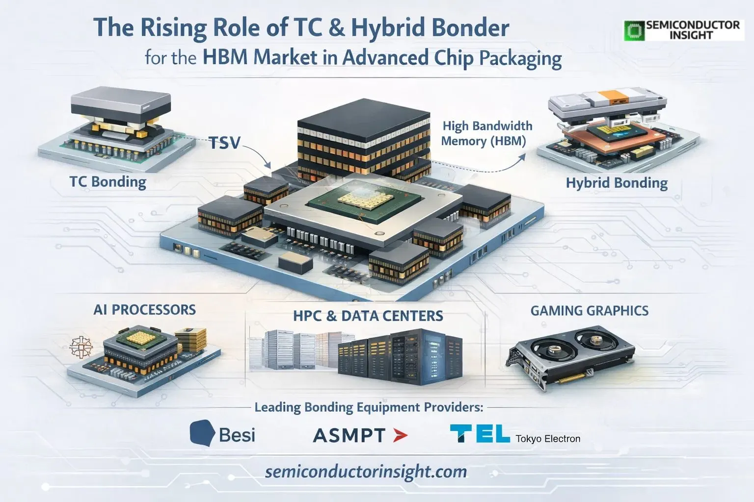
The Rising Role of TC and Hybrid Bonder for HBM Market in Advanced Chip Packaging
High Bandwidth Memory has quickly become a central component in modern semiconductor design, especially in applications such as artificial intelligence processors, advanced graphics cards, and high-performance computing systems. Traditional memory interfaces struggle to keep up with the massive data flow demanded by AI training clusters and large-scale data centers. This is where stacked memory architectures come into play.
HBM works by stacking multiple DRAM layers vertically and connecting them through through-silicon vias (TSVs). The stacking process significantly reduces signal distance, enabling faster data transfer while consuming less power. However, assembling these complex memory stacks requires extremely precise bonding technologies. That is where TC bonding and hybrid bonding technologies become essential.
For instance, modern GPUs designed for AI workloads integrate several HBM stacks placed directly next to the processor die. This architecture is widely used in accelerators such as those powering large language models and high-performance computing systems.
What Exactly Are TC Bonding and Hybrid Bonding Technologies?
Thermo-compression bonding, commonly referred to as TC bonding, is a technique used to attach semiconductor dies together using heat and pressure. It enables extremely strong electrical and mechanical connections, which are necessary when stacking memory dies or connecting memory to logic chips.
Hybrid bonding takes this concept a step further by combining both dielectric bonding and metal-to-metal bonding simultaneously. This method creates ultra-fine interconnects with very low resistance and extremely small pitch sizes.
In advanced packaging environments, hybrid bonding is increasingly used for connecting memory stacks with logic dies in a highly compact architecture. Compared with conventional micro-bump technologies, hybrid bonding offers much higher interconnect density and better signal performance. Because of these advantages, hybrid bonding is emerging as a key enabler of next-generation memory integration.
How Do These Technologies Fit into the HBM Manufacturing Process?
The HBM manufacturing workflow involves several stages that require extremely specialized equipment. First, multiple DRAM dies are thinned and prepared for stacking. These dies are then aligned with micron-level precision before bonding takes place.
TC bonders are typically used in the die stacking stage, where each DRAM layer is connected sequentially to form a vertical stack. Once the stack is completed, the memory module is integrated with a logic processor using interposers or advanced packaging platforms.
Hybrid bonders are increasingly used when extremely fine connections are required between logic chips and memory components. These bonding tools must achieve alignment accuracy within a few hundred nanometers while maintaining high throughput for semiconductor fabrication facilities.
As chip designs become more complex, the need for ultra-precise bonding tools continues to grow. This makes bonding equipment a crucial component in the semiconductor packaging ecosystem.
Which Semiconductor Applications Are Driving Adoption?
Several major technology segments are accelerating the adoption of advanced bonding solutions.
Artificial intelligence processors are among the biggest contributors. AI models require enormous memory bandwidth to process data efficiently, which has made HBM a preferred memory architecture for AI accelerators.
Another important application area is high-performance computing clusters used in scientific simulations and weather modeling. These systems depend heavily on memory bandwidth to process massive datasets.
Gaming graphics processors and data center GPUs also rely heavily on HBM integration. Companies producing high-end graphics cards have increasingly adopted stacked memory to achieve faster rendering speeds and improved performance efficiency.
These developments demonstrate how memory architecture has become just as important as processor design in modern computing platforms.
Which Equipment Manufacturers Are Building These Bonding Systems?
The global semiconductor equipment landscape includes several companies developing bonding solutions for advanced packaging. Firms such as ASMPT, Besi, and Tokyo Electron have introduced specialized systems designed for TC bonding and hybrid bonding applications.
For example, Besi has developed high-precision hybrid bonding platforms capable of handling extremely small interconnect pitches. These systems are designed for wafer-to-wafer and die-to-wafer bonding used in advanced chiplet and memory architectures.
Similarly, Tokyo Electron provides semiconductor manufacturing equipment that supports next-generation packaging technologies. Their bonding tools are designed to maintain alignment accuracy while supporting large-scale production in semiconductor fabrication plants.
The presence of these technology leaders highlights how bonding equipment has become a strategic segment within the semiconductor manufacturing industry.
What Real-World Industry Developments Are Shaping This Market?
Recent developments across the semiconductor ecosystem have significantly increased attention on advanced bonding technologies.
One example is the growing demand for HBM integration in AI processors used in large-scale data centers. Several chip manufacturers have announced next-generation accelerator architectures designed around stacked memory configurations.
Another example comes from semiconductor packaging facilities that are expanding advanced packaging lines specifically to support HBM integration. Many fabrication plants are investing heavily in bonding equipment capable of supporting fine-pitch interconnects.
Meanwhile, chiplet-based architectures are gaining popularity in the semiconductor industry. Instead of building large monolithic chips, manufacturers are increasingly assembling multiple smaller dies into a single package. This approach requires extremely precise bonding technology to ensure performance and reliability.
These industry developments illustrate how bonding technology is becoming a foundational element in advanced semiconductor packaging.
To Know More about the Report, You Can Freely Browse Our Latest Updated Report:
https://semiconductorinsight.com/report/tc-and-hybrid-bonder-for-hbm-market/
Why Is Advanced Packaging Becoming the Center of Semiconductor Innovation?
For decades, semiconductor progress was largely driven by transistor scaling. However, as Moore’s Law approaches physical limits, innovation is increasingly shifting toward packaging technologies.
Stacked memory, chiplet architectures, and heterogeneous integration are redefining how modern chips are built. Instead of relying solely on smaller transistors, manufacturers are combining multiple specialized components within a single package.
Bonding technologies play a critical role in enabling these architectures. Without highly precise bonding tools, it would be nearly impossible to connect multiple chips with the speed and density required for modern computing systems.
This shift explains why equipment used for HBM packaging and advanced bonding has become one of the most closely watched segments in the semiconductor manufacturing ecosystem.

Comments (0)