Market Insights
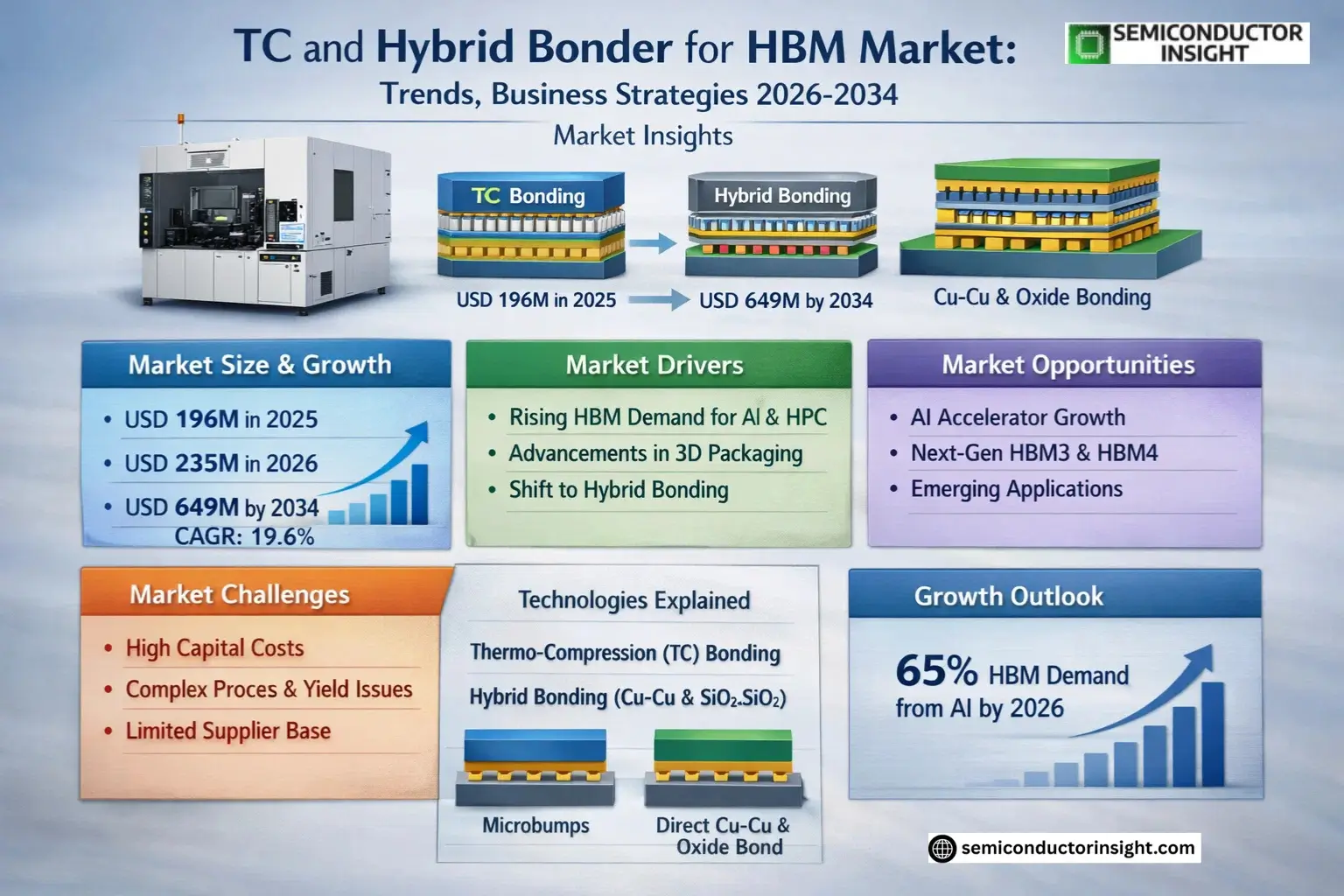
Global TC and Hybrid Bonder for HBM Market size was valued at USD 196 million in 2025. The market is projected to grow from USD 235 million in 2026 to USD 649 million by 2034, exhibiting a CAGR of 19.6% during the forecast period.
TC (Thermo-Compression) bonding is an advanced packaging technology that creates atomic-level interconnects between microbumps and dielectric layers through simultaneous heat (150-300°C) and pressure (5-50kgf) application. Hybrid bonding, a more advanced approach, enables direct copper-to-copper (Cu-Cu) and oxide-to-oxide (SiO₂-SiO₂) connections without intermediate bumps, offering superior density for high-bandwidth memory applications. These technologies are critical enablers for next-generation HBM stacks, with hybrid bonding becoming essential for configurations exceeding 16 layers due to its superior electrical performance and form factor advantages.
MARKET DRIVERS
Growing Demand for High-Bandwidth Memory (HBM) Solutions
The increasing adoption of AI, ML, and high-performance computing applications is driving demand for advanced packaging technologies like TC and Hybrid Bonder for HBM. These solutions enable higher interconnect density and improved thermal performance, critical for next-gen semiconductor devices. Market research indicates a 28% CAGR growth in HBM demand from 2023 to 2028.
Technological Advancements in 3D Packaging
TC and Hybrid Bonder technologies address the challenges of heterogeneous integration in advanced packaging. The shift toward smaller die sizes and higher I/O counts requires precise bonding solutions that these technologies provide, with leading manufacturers reporting yield improvements of up to 15%.
Transition from traditional solder-based interconnects to direct hybrid bonding is creating new opportunities for TC and Hybrid Bonder adoption in HBM manufacturing.
MARKET CHALLENGES
High Capital Investment Requirements
TC and Hybrid Bonder equipment represents a significant capital expenditure, with prices ranging from USD 3-8 million per unit. This creates barriers to entry for smaller semiconductor manufacturers and foundries, particularly in price-sensitive markets.
Other Challenges
Process Complexity and Yield Management
Hybrid bonding for HBM requires ultra-clean environments and nanometer-level precision, with typical process tolerances below 100nm. Maintaining consistent yields above 90% remains challenging even for leading manufacturers.
MARKET RESTRAINTS
Limited Supplier Ecosystem
TC and Hybrid Bonder for HBM Market is currently dominated by a handful of equipment manufacturers, creating supply chain vulnerabilities. This limited competition also slows price erosion, with average system costs declining only 4-6% annually despite increasing volumes.
MARKET OPPORTUNITIES
Emerging Applications in AI Accelerators
The rapid growth of AI accelerator chips, which extensively utilize HBM memory stacks, presents significant opportunities for TC and Hybrid Bonder adoption. Industry analysts project AI-related HBM demand to account for 65% of total TC and Hybrid Bonder system shipments by 2026.
TC and Hybrid Bonder for HBM Market Trends
Accelerated Adoption of Advanced Packaging Technologies
TC and Hybrid Bonder for HBM Market is witnessing rapid growth driven by increasing demand for high-bandwidth memory in AI and data center applications. Through-Silicon Via (TC) bonding remains dominant for mid-range HBM stacks due to its cost efficiency and proven reliability in semiconductor manufacturing processes. Hybrid bonding is gaining traction for high-density packaging requirements, particularly in next-generation HBM3/3E and HBM4 modules.
Other Trends
Equipment Pricing and Market Segmentation
TC bonding machines for HBM maintain an average unit price of USD 1.2 million, with manufacturers achieving gross margins around 45%. The hybrid bonding equipment segment remains in early commercialization phase, with major OEMs planning volume shipments by late 2025.
Technology Differentiation Between TC and Hybrid Bonding
TC bonding continues to dominate for HBM2E and below, offering temperature ranges of 150-300°C and pressure between 5-50kgf. Hybrid bonding technology provides superior interconnect density through copper-copper and oxide-oxide bonding, making it ideal for 16+ layer HBM configurations. Leading semiconductor manufacturers are investing heavily in both technologies to maintain production flexibility.
Regional Market Developments
Asia-Pacific accounts for the majority of production capacity, with South Korea and Taiwan leading in HBM manufacturing infrastructure. North American and European markets are focusing on R&D for next-generation bonding technologies, with several joint development programs between equipment manufacturers and IDMs.
Competitive Landscape Evolution
The market remains concentrated among key players including HANMI Semiconductor, ASMPT, and SEMES, who collectively hold significant market share. Recent technological advancements have intensified competition in hybrid bonding solutions, with multiple suppliers expected to introduce commercial systems in 2025.
COMPETITIVE LANDSCAPE
Key Industry Players
Technological Advancements Driving Market Consolidation
TC and Hybrid Bonder for HBM Market is dominated by specialized semiconductor equipment manufacturers, with HANMI Semiconductor and ASMPT leading in revenue share. These companies benefit from patented bonding technologies and long-term partnerships with major memory manufacturers like Samsung and SK Hynix. The top five players collectively control over 65% of the market, with technological barriers preventing new entrants from gaining significant traction. Hybrid bonding solutions remain concentrated among European and Asian manufacturers capable of nanometer-scale precision engineering.
Niche players such as Tazmo and Shibaura Mechatronics compete through regional supply chains and application-specific solutions for mid-layer HBM production. The market sees increasing R&D investments from Japanese and Korean firms targeting hybrid bonding automation, while Chinese manufacturers are rapidly developing TC bonder alternatives to reduce import dependence. Equipment differentiation focuses on throughput (units/hour), alignment accuracy (±0.5μm), and thermal control stability (±1°C).
List of Key TC and Hybrid Bonder for HBM Companies Profiled
- HANMI Semiconductor
- ASMPT
- SEMES
- Hanwha Semitech Co., Ltd
- Yamaha Robotics (SHINKAWA)
- Besi
- Tazmo Co., Ltd.
- Shibaura Mechatronics
- Tokyo Electron Limited
- Kulicke & Soffa
- Ultra Tec Manufacturing Inc.
- Applied Materials
- ASM International
- EV Group (EVG)
- SUSS MicroTec
Segment Analysis:
| Segment Category | Sub-Segments | Key Insights |
| By Type |
|
TC Bonder currently dominates due to its maturity and cost advantages for low-to-mid layer HBMs. The Hybrid Bonder segment is gaining prominence as:
|
| By Application |
|
HBM3/3E represents the most dynamic growth segment with:
|
| By End User |
|
Memory Manufacturers are the primary technology adopters due to:
|
| By Technology Readiness |
|
Mature TC Bonding maintains strong market position while hybrid bonding evolves:
|
| By Equipment Provider |
|
Semiconductor Capital Equipment Leaders dominate due to:
|
Regional Analysis: TC and Hybrid Bonder for HBM Market
Samsung and SK Hynix are driving TC bonder adoption through vertical integration strategies, developing proprietary bonding processes optimized for HBM stacks. Their captive production facilities enable rapid implementation of bonding technology advancements.
TSMC’s CoWoS platform has established Taiwan as a hybrid bonding hub, with advanced interposer technologies enabling high-density HBM integration. Local equipment suppliers are developing bonders with sub-micron alignment accuracy for 3D IC applications.
Japanese manufacturers provide critical TC and hybrid bonder components including precision stages and thermal control systems. Their bonding equipment supports the stringent cleanliness and stability requirements of HBM production lines.
Domestic equipment makers are making progress in TC bonder development, supported by government funding. While trailing leaders in yield rates, Chinese suppliers are becoming credible alternatives for mature node HBM production.
North America
North America plays a critical role in TC and hybrid bonder R&D, with semiconductor equipment companies developing next-generation platforms for HBM manufacturing. Silicon Valley remains the center of bonding technology innovation, particularly in materials science and process control algorithms. Leading logic chip designers collaborate with memory partners in Asia to co-optimize bonding processes for HBM interfaces. The region benefits from strong university research programs focused on interconnect reliability and thermal management challenges in advanced packaging.
Europe
European equipment suppliers specialize in niche bonding technologies for automotive and industrial HBM applications. The region excels in developing robust TC bonding solutions meeting stringent quality requirements. German and Dutch companies provide critical subsystems for hybrid bonders, including high-precision alignment modules. European semiconductor materials firms supply advanced underfills and adhesives optimized for HBM thermal cycling reliability.
Middle East & Africa
The region is emerging as a strategic location for HBM assembly and test facilities, attracting investments in TC bonding infrastructure. Government initiatives aim to develop local semiconductor ecosystems, with bonding technology transfer partnerships established with Asian equipment providers. Regional demand grows for HBM-based AI accelerators in data center applications.
South America
While not a major TC bonder manufacturing hub, South America sees increasing adoption of HBM technologies for hyperscale computing applications. Local packaging houses are upgrading capabilities to handle bonded memory stacks, particularly for AI/ML accelerator modules. The region benefits from proximity to North American design centers driving HBM adoption.
Report Scope
This market research report provides a comprehensive analysis of the TC and Hybrid Bonder for HBM Market, covering the forecast period 2025–2032. It offers detailed insights into market dynamics, technological advancements, competitive landscape, and key trends shaping the industry.
Key focus areas of the report include:
- Market Overview: The report begins with an overview outlining its current market scenario, key growth indicators, and industry transformation drivers. It discusses macroeconomic factors, demand–supply balance, regulatory landscape, and the strategic role of semiconductors in powering advancements across industries such as automotive, telecommunications, consumer electronics, and industrial automation.
- Market Size & Forecast: Historical data and future projections for revenue, unit shipments, and market value across major regions and segments.
- Segmentation Analysis: Detailed breakdown by product type, technology, application, and end-user industry to identify high-growth segments and investment opportunities.
- Regional Insights: Insights into market performance across North America, Europe, Asia-Pacific, Latin America, and the Middle East & Africa, including country-level analysis where relevant.
- Competitive Landscape: Profiles of leading market participants, including their product offerings, R&D focus, manufacturing capacity, pricing strategies, and recent developments such as mergers, acquisitions, and partnerships.
- Technology Trends & Innovation: Assessment of emerging technologies, integration of AI/IoT, semiconductor design trends, fabrication techniques, and evolving industry standards.
- Market Drivers & Restraints: Evaluation of factors driving market growth along with challenges, supply chain constraints, regulatory issues, and market-entry barriers.
- Stakeholder Insights: Insights for component suppliers, OEMs, system integrators, investors, and policymakers regarding the evolving ecosystem and strategic opportunities.
Primary and secondary research methods are employed, including interviews with industry experts, data from verified sources, and real-time market intelligence to ensure the accuracy and reliability of the insights presented.
FREQUENTLY ASKED QUESTIONS:
What is the current market size of TC and Hybrid Bonder for HBM Market?
-> TC and Hybrid Bonder for HBM Market size was valued at USD 196 million in 2025. The market is projected to grow from USD 235 million in 2026 to USD 649 million by 2034, exhibiting a CAGR of 19.6% during the forecast period.
What is the projected CAGR for the TC and Hybrid Bonder for HBM Market?
-> The market is projected to grow at a CAGR of 19.6% during the forecast period (2025-2032).
Which key companies operate in TC and Hybrid Bonder for HBM Market?
-> Key players include HANMI Semiconductor, ASMPT, SEMES, Hanwha Semitech Co., Ltd, Yamaha Robotics (SHINKAWA), and Besi.
What are the key growth drivers?
-> Key growth drivers include increasing demand for high-layer HBMs (16+ layers), performance breakthroughs in hybrid bonding technology, and advancements in semiconductor packaging.
Which region dominates the market?
-> Asia-Pacific is the dominant market, with key contributions from countries like China, Japan, and South Korea.
Get Sample Report PDF for Exclusive Insights
Report Sample Includes
- Table of Contents
- List of Tables & Figures
- Charts, Research Methodology, and more...