TGV Wafers Powering Next-Gen RF Systems: Surge in Hermetic Packaging, MEMS Integration, and LIDE Etching Fuels 9.6% CAGR Growth Through 2032
As demand for smaller, faster, and more reliable RF components escalates across industries such as telecommunications, automotive, aerospace, and consumer electronics, the spotlight is now firmly on Through Glass Via (TGV) wafers. TGV technology, once a niche packaging solution, is gaining traction for its ability to support high-frequency, low-loss, and compact integration of radio frequency (RF) components.
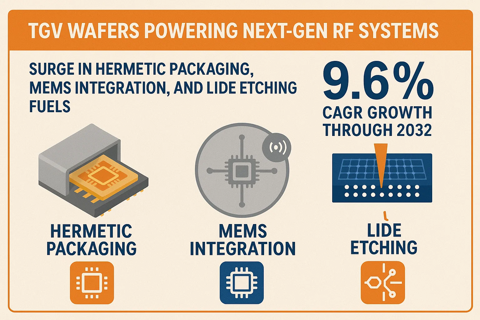
In 2024, the global TGV wafer for RF applications market was valued at US$ 156.8 million, and it is projected to almost double to US$ 298.7 million by 2032, growing at a robust CAGR of 9.6% during the forecast period (2025–2032).
Access Your Free Sample Report- Through Glass Via (TGV) Wafer for RF Applications Market
Understanding Through Glass Via (TGV) Technology
Through Glass Vias (TGVs) are microscopic holes or vias etched through glass substrates and filled with conductive materials like copper. They provide vertical interconnections in wafer-level packaging and are particularly suited to RF and mmWave signal transmission due to their superior electrical insulation, high dimensional stability, and low dielectric loss.
Key Benefits of TGVs in RF Applications:
- Excellent electrical performance: Low signal loss and low dielectric constant.
- High precision: Enables fine pitch interconnects with excellent dimensional control.
- Thermal and chemical stability: Essential for harsh environments and extended operational life.
- Miniaturization: Facilitates 3D integration and reduced form factor.
Recent Technological Developments in TGV Wafer Packaging
The TGV industry is at a turning point, driven by a wave of cutting-edge advancements in materials science, process engineering, and integration methodologies. Here are the most impactful developments reshaping the landscape of TGV wafers for RF applications:
- Wafer-Level Hermetic RF Packaging with Transient Liquid Phase Bonding
One of the most revolutionary shifts is the integration of Cu/Ni/Sn-based transient bonding with copper-filled TGVs to create hermetic RF filter modules. These advanced 3D wafer-level packages enable:
- Vacuum encapsulation for sensitive RF MEMS devices.
- Low insertion loss across RF signal paths.
- High-yield solder-ball connectivity, crucial for high-frequency reliability.
This innovation enables mass production of compact, high-performance RF modules, aligning perfectly with the needs of 5G/6G infrastructure and consumer electronics.
- TGV Packaging for MEMS-Based RF Sensors
Recent breakthroughs in packaging motion sensors and MEMS gyroscopes have utilized TGV-based glass caps fabricated using:
- Laser ablation
- Glass reflow
- Powder blasting
These methods achieve sub-30 µm via diameters and hermetic seals for high vacuum stability, leading to:
- High Q-factors (>220,000) in MEMS gyroscopes.
- Improved shock resistance and lifetime reliability.
- Enhanced frequency stability, crucial for mmWave applications.
Such integration of MEMS and RF modules through TGVs opens new frontiers in aerospace, autonomous vehicles, and defense systems.
- Adoption of Laser-Induced Deep Etching (LIDE) Technology
The development of Laser-Induced Deep Etching (LIDE) is a significant game changer. LIDE allows the etching of:
- Highly uniform, crack-free vias
- Vias as narrow as 10 µm
- Depths exceeding 400 µm
This ensures higher interconnect densities, allowing over 8000 TGVs per wafer, and supports frequencies above 150 GHz, making TGVs ideal for 6G, satellite communication, and AI-integrated RF modules.
- Thermal Management Integration within TGV Substrates
As RF systems become more power-hungry, thermal design is becoming as critical as signal integrity. TGV wafers are now being developed with:
- Embedded thermal spreaders
- Microfluidic cooling channels
- High thermal conductivity glass
These innovations improve heat dissipation, prolonging module life and maintaining performance in extreme temperature environments like automotive radar or aerospace radomes.
Global Momentum and Regional Developments
Asia-Pacific: Driving the Production Engine
The Asia-Pacific region continues to dominate TGV wafer production, primarily led by:
- China: Foxconn and other contract manufacturers are ramping up TGV-based RF antenna module production for smartphones and smart wearables.
- Taiwan: TSMC and ASE are investing heavily in TGV-based 3D IC packaging lines.
- South Korea: SK Hynix and Samsung are integrating TGV wafers in advanced HBM and mmWave transceiver modules.
These developments are supported by strong government incentives for advanced semiconductor packaging technologies.
North America and Europe: Innovation Hubs for RF and Aerospace
The U.S. Department of Defense is now including TGV compatibility in procurement specifications for secure communications and high-frequency radar modules. European initiatives, particularly under Horizon Europe, are funding TGV-based packaging for automotive radar and satellite-on-chip applications.
Recent installations in Germany, Sweden, and the Netherlands highlight Europe’s growing commitment to this critical packaging technology.
Download Sample Report PDF- Through Glass Via (TGV) Wafer for RF Applications Market
Industry Applications Gaining Traction
- 5G and Emerging 6G Networks
The core of modern telecom is built on low-loss, high-frequency signal transmission. TGVs offer:
- Exceptional signal integrity in antenna-in-package (AiP) modules.
- Integration of beamforming arrays for MIMO antennas.
- Higher packaging density, essential for small cell base stations.
- Automotive Radar & V2X Communication
Radar and LiDAR systems for autonomous vehicles require:
- Compact RF packages.
- Excellent thermal resistance.
- Long-term vacuum reliability.
TGV wafers provide hermetic, thermally stable enclosures that meet stringent automotive-grade reliability standards.
- Aerospace & Defense Electronics
The aerospace sector benefits from TGV’s:
- Lightweight structure.
- High thermal stability.
- Resistance to outgassing in vacuum.
Applications include satcom transceivers, military-grade radar, and inter-satellite communication systems.
- AI-Integrated RF and Sensor Modules
With the rise of edge AI and smart sensing, RF packaging needs to handle:
- Multiple signal domains (RF + digital + optical).
- High-density routing within minimal space.
TGV wafers provide the interconnect backbone for such highly integrated modules.
Market Challenges
While the TGV market offers exciting opportunities, several technical and economic hurdles remain:
- Manufacturing Complexity
TGV wafer processing involves:
- Ultra-precise via alignment.
- Cleanroom-level contamination control.
- Fragile handling due to thinness (~150 µm).
These steps increase production costs and limit throughput.
- Brittleness of Glass
Despite its benefits, glass is inherently brittle. Innovations such as edge reinforcement and encapsulation coatings are being developed but add to cost and design complexity.
- Supply Chain Bottlenecks
The availability of:
- TGV-capable glass substrates.
- Specialized etching and metallization equipment.
- Skilled labor for yield optimization
…is currently limited to a few regions and companies, making scalability a concern.
Competitive Landscape
Several players are pioneering the future of TGV wafer technology:
| Company | Contribution |
| LPKF | LIDE technology provider for fine TGV etching. |
| Corning | Advanced glass substrates for high-frequency applications. |
| ASE Group | Large-scale packaging with Cu-filled TGVs for RF and HBM modules. |
| TSMC | Exploring hybrid bonding with TGV interposers in 3D ICs. |
| Kyocera | Development of hermetic TGV packages for automotive and defense markets. |
Forecast and Growth Outlook (2025–2032)
With a CAGR of 9.6%, the TGV wafer market is poised for rapid expansion. Growth drivers include:
- Rising data traffic and RF bandwidth demand.
- Increasing miniaturization in consumer devices.
- Expansion of 5G/6G infrastructure and satellite communication.
- Broader use of MEMS-based RF sensors and automotive radar.
Market Projections by 2032:
- North America: US$ 85.4 million
- Asia-Pacific: US$ 144.3 million
- Europe: US$ 47.5 million
- ROW: US$ 21.5 million
Click Here To Download Full Sample Report- Through Glass Via (TGV) Wafer for RF Applications Market
The Through Glass Via (TGV) wafer for RF applications market is entering a transformative phase. Fueled by strong demand from 5G/6G, aerospace, automotive, and AI sectors, and propelled by innovations in etching, bonding, and thermal integration, TGV wafers are redefining what’s possible in RF packaging.
Despite challenges around manufacturing complexity and supply chain constraints, ongoing breakthroughs in LIDE technology, wafer-level hermetic packaging, and MEMS integration ensure a promising trajectory. As the market grows from US$ 156.8 million in 2024 to US$ 298.7 million by 2032, TGV wafers will increasingly become the backbone of next-gen RF, mmWave, and high-density systems.
Comments (0)