
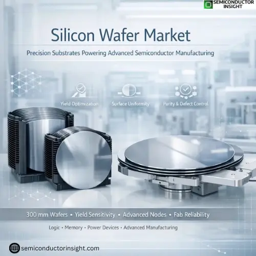
Technology Development and Capacity Pressure in Silicon Wafer Market
Setting the Stage Where Every Chip Begins?
Every semiconductor device, regardless of complexity, traces its origin to a silicon wafer. Before logic circuits, memory cells, or power devices take shape, the wafer establishes the physical and electrical foundation upon which performance is built. Silicon wafer market is therefore not just a materials segment it is a strategic pillar of the global semiconductor industry.
As chip architectures advance and manufacturing nodes continue to shrink, wafer quality, flatness, and purity have become decisive factors influencing yield, cost efficiency, and device reliability.
Market Definition and Industry Role
Silicon wafer market covers the production and supply of monocrystalline and, to a lesser extent, polycrystalline silicon substrates used in semiconductor fabrication. These wafers are processed through multiple steps including slicing, polishing, cleaning, and inspection before entering wafer fabs.
Wafers are categorized by diameter most notably 200 mm and 300 mm with 300 mm wafers dominating advanced logic and memory production due to their superior cost-per-chip efficiency. Smaller diameters remain relevant for power electronics, analog devices, and legacy process nodes.
Technology Evolution Driving Market Complexity
The market has moved far beyond simple volume growth. As semiconductor manufacturers adopt advanced process nodes and three-dimensional architectures, wafer specifications have tightened significantly. Requirements related to surface roughness, thickness uniformity, and defect density are becoming more stringent.
This evolution has elevated wafer manufacturing into a precision engineering discipline, where marginal improvements translate directly into higher yields at the fab level. As a result, wafer suppliers are investing heavily in metrology, crystal growth optimization, and polishing technologies.
Capacity Expansion and Supply Alignment
Silicon wafer market operates on long investment cycles. Capacity expansions require years of planning, high capital expenditure, and close coordination with semiconductor manufacturers. Recent industry conditions have underscored the importance of supply reliability, as wafer shortages can constrain fab utilization even when downstream demand is strong.
Long-term supply agreements between wafer producers and chip manufacturers have become more common, helping stabilize pricing and ensure predictable access to critical substrates. This shift reflects the strategic value of wafers within the broader semiconductor ecosystem.
Pricing Dynamics and Cost Structure
Silicon wafer pricing is influenced by several factors, including raw silicon availability, energy costs, capital intensity, and yield optimization. Wafers command value based on performance and consistency rather than just volume, in contrast to commoditized materials.
Advanced wafers designed for leading-edge nodes typically involve premium pricing due to their complex manufacturing requirements. At the same time, mature-node wafers maintain steady demand, creating a dual-track market structure that balances innovation with stability.
Regional Manufacturing and Trade Considerations
Wafer production is geographically concentrated, with manufacturing hubs aligned closely to major semiconductor fabrication regions. Trade policies, export controls, and regional self-sufficiency initiatives are increasingly shaping investment decisions within the market.
Governments supporting domestic semiconductor manufacturing are also indirectly influencing wafer supply chains through incentives, infrastructure development, and research funding. This has made wafer production a strategic consideration within national semiconductor roadmaps.
You can freely browse our most recent updated report to learn more about it before scrolling further:
https://semiconductorinsight.com/report/silicon-wafer-market/
Quality Control and Yield Sensitivity
In semiconductor manufacturing, small defects can lead to significant yield losses. As device geometries shrink, the tolerance for wafer imperfections narrows further. This places intense emphasis on inspection, defect mapping, and process repeatability.
Wafer suppliers that consistently deliver high-quality substrates gain long-term partnerships, while those unable to meet evolving specifications risk displacement. Quality assurance has therefore become a central competitive factor rather than a supporting function.
Sustainability and Manufacturing Efficiency
Environmental considerations are gaining relevance in wafer manufacturing. Energy consumption, water usage, and chemical handling are under increasing scrutiny. Suppliers are responding by improving process efficiency, recycling materials, and reducing waste without compromising quality.
Sustainability efforts are also aligned with cost reduction objectives, making operational efficiency a shared priority for both wafer producers and semiconductor manufacturers.
Competitive Landscape and Strategic Positioning
Silicon wafer market is characterized by a limited number of highly specialized players with deep technical expertise. Competitive advantage is built through scale, process know-how, and long-standing customer relationships.
Strategic investments are focused on expanding 300 mm wafer capacity, enhancing advanced polishing capabilities, and supporting next-generation semiconductor technologies. Collaboration with chipmakers during early process development phases is becoming increasingly common.
In the years to come, the market for silicon wafers is anticipated to expand in tandem with the demand for semiconductors in applications related to computer, automotive, industrial automation, and communication. Growth will be defined not only by volume, but by precision, consistency, and integration into advanced manufacturing flows.

Comments (0)