
Single Element Atomic Absorption Spectrophotometers Market: The Atomic Gatekeepers of Chip Fabrication
Semiconductor manufacturing operates at scales where a single stray metal atom can derail an entire production run. Single element atomic absorption spectrophotometers deliver the pinpoint accuracy needed to keep wafers free of contaminants that would otherwise destroy device performance.
These instruments shine a specific wavelength of light through an atomized sample and measure exactly how much is absorbed by atoms of one target element. Because each analysis focuses on a single metal, the technique achieves unmatched sensitivity and reliability in environments where even parts-per-trillion impurities matter.
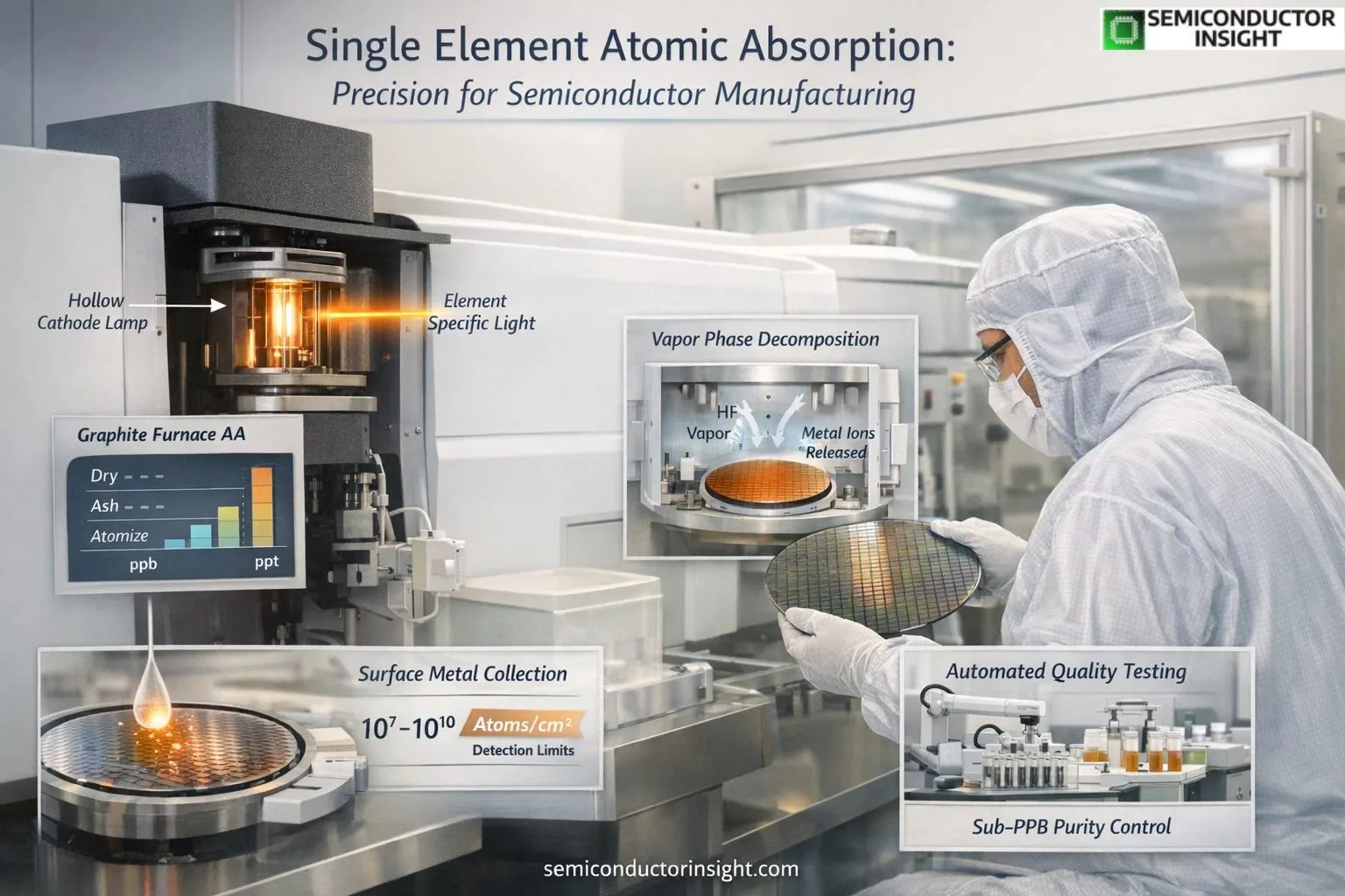
- The heart of every measurement is the hollow cathode lamp. Each lamp contains a cathode made from the pure element being tested iron, copper, sodium, or nickel, for example.
- When current flows, the lamp emits sharp spectral lines unique to that element. This element-specific light passes through the sample vapor, and only atoms of the matching element absorb it.
- The amount of absorption follows Beer’s law, allowing direct calculation of concentration. In a cleanroom setting, technicians swap lamps in minutes to switch from checking iron in ultra-pure water to verifying copper levels in a photoresist
- The approach eliminates interference from other metals that plague multi-element techniques, giving fabs the confidence to release materials for the next process step.
Get the complete report through the link below: https://semiconductorinsight.com/report/global-single-element-atomic-absorption-spectrophotometer-market/
Vapour Phase Decomposition Elevates Surface Inspection to New Levels
When engineers need to scan an entire 300-millimeter wafer for invisible metal films, they turn to vapour phase decomposition. The wafer sits in a sealed chamber while hydrofluoric acid vapor gently etches away the native oxide layer, releasing trapped metal ions into tiny acid droplets. A scanning droplet then collects everything from the surface and the concentrated sample feeds straight into the atomic absorption spectrophotometer.
This combination routinely reaches detection limits of 10^7 to 10^10 atoms per square centimeter orders of magnitude below what bare instruments can achieve. Iron and nickel, two of the most damaging contaminants for gate oxide integrity, show up clearly even when present in quantities smaller than a billionth of a monolayer. Fabs processing advanced logic and power devices rely on this workflow daily to confirm that cleaning baths and deposition chambers remain within strict purity windows.
Graphite Furnace Variants Deliver Sub-Parts-Per-Trillion Performance
- For the most demanding applications, graphite furnace atomic absorption takes the technique further.
- Instead of a flame, the sample is placed inside a tiny graphite tube that heats in precise stages drying, ashing, and atomizing under an inert gas flow.
- The concentrated cloud of atoms stays inside the optical path longer, boosting sensitivity dramatically. In practice, this lets quality team’s measure sodium or calcium in process chemicals at levels that once required days of sample preparation.
- Modern furnace systems also automate multiple injections and background correction, reducing human error in around-the-clock fab operations.
- When a new high-k dielectric process rolls out, engineers use these instruments to qualify every incoming batch of precursor chemicals before they touch a single wafer.
Keeping Process Chemicals and Ultra-Pure Water on Specification
Every liter of ultra-pure water and every drum of etchant or slurry passes through rigorous testing. Single element atomic absorption spectrophotometers sit at the heart of these qualification loops. A small aliquot is nebulized, and the instrument quickly reports the exact concentration of critical metals such as aluminum, potassium, or zinc. Results feed directly into statistical process control charts; any spike triggers an immediate hold on the chemical lot.
In one recent high-volume logic fab expansion, the ability to verify iron below 0.01 parts per billion in incoming hydrogen peroxide prevented yield excursions that would have cost millions in scrapped wafers. The same instruments monitor recycled solvents, ensuring that reclaim streams meet the same purity standards as virgin material and supporting the industry’s drive toward lower chemical consumption.
Seamless Fit into High-Volume Manufacturing Workflows
- Today’s 300-millimeter production lines integrate these spectrophotometers into automated sample-handling stations.
- Robots deliver pre-treated droplets or diluted solutions, the instrument runs the analysis, and results stream into the factory’s manufacturing execution system within minutes.
- Technicians monitor dashboards that flag any element trending toward its control limit, allowing maintenance teams to clean tools or replace filters before contamination spreads.
- This closed-loop approach has become standard for both memory and foundry operations pushing into angstrom-scale features.
Whether qualifying a new EUV photoresist or verifying backside cleaning on bonded wafers, the single element atomic absorption spectrophotometer remains the trusted referee that keeps billion-dollar fabs running at peak yield. Its combination of simplicity, specificity, and proven sensitivity continues to underpin the relentless progress of semiconductor technology.

Comments (0)