
Precision Oxide Polishing Top Trends in the Shallow Trench Isolation Slurries Market
In advanced semiconductor fabrication, the ability to isolate millions of transistors on a single silicon wafer is essential for reliable device performance. One of the key technologies used to achieve this isolation is Shallow Trench Isolation (STI), where narrow trenches are etched into silicon and filled with dielectric material to electrically separate adjacent devices. During this process, specialized chemical mechanical planarization materials known as STI slurries are used to polish and flatten the wafer surface with extremely high precision.
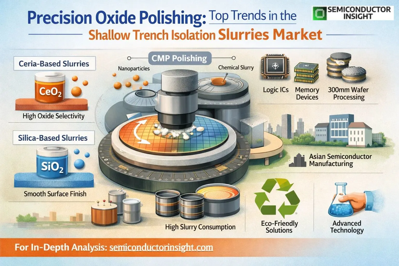
STI slurries typically combine abrasive particles such as cerium oxide (ceria) or colloidal silica with chemical additives that control polishing rates and surface selectivity. These materials allow manufacturers to remove excess oxide while protecting underlying layers like silicon nitride. High selectivity is critical because even minor surface defects can lead to chip failure in advanced nodes used for processors, AI accelerators, and memory devices.
As semiconductor technology continues to shrink below 7-nanometer nodes, the demand for extremely uniform planarization materials has increased significantly. Today, STI slurries are essential consumables used in the front-end-of-line manufacturing steps of integrated circuits.
Chemical Composition and Process Engineering
STI slurries are engineered to balance mechanical abrasion with chemical reactions on the wafer surface. The abrasive particles are usually extremely small, often below 100 nanometers in diameter, allowing precise control over polishing rates without damaging the wafer.
Two common slurry chemistries dominate this process:
- Ceria-based slurries are widely used because they offer very high oxide-to-nitride selectivity during polishing. Studies show that ceria abrasives can achieve selectivity levels up to 100 times higher than traditional silica slurries under certain conditions.
- Silica-based slurries, on the other hand, are preferred for applications that require minimal surface defects and smoother wafer finishes.
In a typical CMP process, polishing pads rotate at controlled speeds while slurry flows across the wafer surface. Adjustments in pressure, rotational speed, and chemical concentration influence removal rates and surface uniformity. Even small variations in slurry chemistry can change polishing efficiency by several percent, making formulation control extremely important.
Semiconductor Manufacturing Demand and Production Trends
The rapid expansion of the semiconductor industry has increased the use of CMP materials across global fabrication plants. Asia-Pacific currently dominates semiconductor production, accounting for approximately 78% of global chip manufacturing output, making it the largest consumer of STI slurry materials.
In terms of device applications, logic integrated circuits represent around 40% of STI slurry usage, while memory devices such as DRAM and NAND flash account for about 35%. The remaining demand comes from sensors, MEMS devices, and specialized microelectronics.
Advanced wafer fabrication plants operating with 300-mm wafers process thousands of wafers per day, and each wafer can require multiple CMP polishing steps. As a result, slurry consumption in large semiconductor fabs can reach several tons of material annually.
For a more thorough report, please contact us using our most recent report: https://semiconductorinsight.com/report/shallow-trench-isolation-sti-slurries-market/
Major Companies Driving Innovation
- The STI slurry ecosystem is led by specialized semiconductor materials companies that invest heavily in research and process optimization.
- One of the most influential companies is Cabot Microelectronics (now part of Entegris), which holds roughly 35% share of the silica-based CMP slurry segment. Its proprietary formulations focus on particle uniformity and defect reduction during advanced node manufacturing.
- Fujimi Corporation is another major supplier known for high-purity silica slurries used in dielectric planarization. Its PLANERLITE slurry platform is specifically designed for silicon dioxide polishing in STI and interlayer dielectric processes.
- Merck KGaA, through its semiconductor materials division, develops customized oxide CMP slurries used in leading foundries for advanced logic nodes and packaging technologies.
- Other important companies include Resonac (formerly Hitachi Chemical), AGC Inc., Dongjin Semichem, Soulbrain, and Fujifilm Holdings. Together, several leading suppliers collectively control more than 45% of the global STI slurry supply chain, reflecting the highly specialized nature of this industry.
Technology Outlook and Material Advancements
Reducing defectivity while enhancing environmental sustainability is a growing emphasis of future STI slurry development. Manufacturers are exploring recyclable slurry systems and formulations that reduce chemical waste generated during polishing.
Some companies have introduced slurry packaging systems that reduce waste generation by 30%, while others are experimenting with bio-based stabilizers and lower-carbon manufacturing processes.
In parallel, advances in nanoparticle engineering are enabling better particle size distribution control, which is crucial for next-generation semiconductor devices with extremely tight surface tolerances.
As semiconductor architectures continue evolving toward smaller nodes and more complex 3D structures, high-performance CMP slurry technologies will remain critical materials enabling precision manufacturing in the global electronics industry.

Comments (0)