
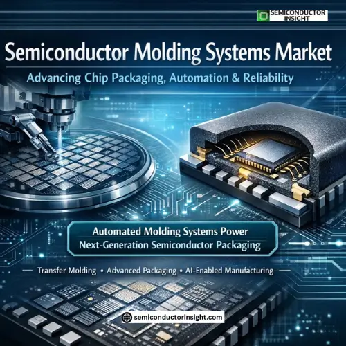
Semiconductor Molding Systems Market Boosts Advanced Chip Packaging
Semiconductor packaging has become a critical stage in modern chip manufacturing, ensuring that delicate integrated circuits are protected from environmental stress, mechanical damage, and thermal fluctuations. Semiconductor Molding Systems Market plays a vital role in this process by enabling precise encapsulation of semiconductor devices using epoxy compounds and advanced molding techniques.
With semiconductor devices now integrated into nearly every electronic product from smartphones and laptops to electric vehicles and AI infrastructure the demand for reliable packaging technologies continues to increase. Semiconductor molding systems ensure that chips maintain durability, electrical stability, and performance reliability across demanding applications.
Modern molding equipment has evolved significantly in recent years. Today’s systems are designed with automated cavity control, vacuum sealing capabilities, and precision temperature regulation to maintain packaging consistency across large production volumes. As semiconductor components continue shrinking in size while increasing in complexity, the need for advanced molding systems has intensified.
Role of Encapsulation in Semiconductor Reliability
- Encapsulation is one of the most important steps in semiconductor packaging. During the molding process, integrated circuits are sealed within protective polymer materials that shield them from moisture, contamination, and mechanical stress.
- Packaging technologies using molding systems are capable of improving device durability by reducing thermal stress and preventing electrical leakage. In high-performance electronics, this process significantly improves long-term reliability.
- Several semiconductor packages depend on molding systems, including QFN packages, BGA packages, and power modules. Wafer-level packaging alone accounts for nearly 40 packaging installations across advanced semiconductor production facilities worldwide. Additionally, ball grid array packaging contributes close to 30 packaging deployments across chip manufacturing lines.
- As semiconductor devices become thinner and more compact, molding technologies must maintain uniform material distribution across micro-scale cavities, ensuring structural integrity without compromising performance.
You can freely browse our most recent updated report to learn more about it before scrolling further:
https://semiconductorinsight.com/report/semiconductor-molding-systems-market/
Automation in Transfer Molding Equipment
Transfer molding remains the most widely adopted process in semiconductor encapsulation. It enables molten epoxy compound to flow into mold cavities that contain semiconductor dies and bonding wires.
This technology currently represents close to 46 installations across semiconductor molding systems used in packaging facilities. Compression molding follows with roughly 31 installations, while injection molding systems account for about 15.
Automation has significantly improved the efficiency of transfer molding operations. Multi-cavity systems allow manufacturers to process dozens of semiconductor units simultaneously, reducing production cycles and improving yield consistency. Over 60 advanced semiconductor packaging plants now operate automated multi-cavity molding platforms to increase throughput and minimize downtime.
These automated systems also integrate robotic wafer handling and real-time pressure monitoring to maintain consistent molding quality.
Growth of Fully Automated Systems
Automation is becoming a defining trend in semiconductor manufacturing equipment. Fully automated molding systems dominate semiconductor packaging facilities due to their ability to maintain precise molding pressure, temperature stability, and repeatable production cycles.
Automatic molding equipment currently represents approximately 55 installations across semiconductor molding production lines, while semi-automatic systems account for about 30 installations and manual equipment contributes around 15.
Automated systems help semiconductor manufacturers achieve higher packaging yields and reduce material waste. They also allow production lines to operate continuously with minimal operator intervention, improving operational efficiency.
Many modern semiconductor molding systems now include AI-enabled process monitoring, predictive maintenance sensors, and automated defect detection modules that identify packaging inconsistencies before final assembly.
Advanced Packaging Technologies and Miniaturization
- The semiconductor industry continues to push toward smaller, faster, and more energy-efficient chips. As device geometries shrink, packaging technologies must adapt to support higher density components and improved thermal performance.
- Miniaturization has accelerated the adoption of advanced packaging methods such as fan-out wafer-level packaging, 3D integration, and chiplet architectures. These technologies require molding systems capable of extremely precise encapsulation to avoid voids or micro-defects within semiconductor packages.
- More than 41 semiconductor packaging facilities have recently integrated enhanced thermal dissipation modules within molding lines to improve heat management and device longevity. These systems improve heat transfer efficiency by nearly 19 while extending chip lifespan across high-performance electronics.
- Advanced packaging is especially important for power electronics, automotive chips, and high-performance computing devices where thermal stability directly impacts reliability.
Regional Overview of Manufacturing Hubs
Asia-Pacific dominates global semiconductor molding system installations due to its strong semiconductor manufacturing ecosystem. The region accounts for roughly 45-56% share of global semiconductor molding equipment usage, supported by large packaging clusters in China, Taiwan, Japan, and South Korea.
Several countries in the region host hundreds of semiconductor packaging plants and outsourced semiconductor assembly and test facilities. These manufacturing hubs collectively account for nearly 70 semiconductor molding equipment installations worldwide, reinforcing the region’s leadership in chip packaging infrastructure.
North America represents the second major hub for semiconductor molding technologies, contributing close to 25% share of global installations. The region benefits from strong semiconductor R&D investments, advanced chip design infrastructure, and rising demand for high-performance computing and automotive electronics.
Growing investments in domestic semiconductor manufacturing and advanced packaging facilities are further expanding the adoption of molding systems across fabrication and assembly plants.

Comments (0)