
Semiconductor Manufacturing Landscape of the DDIC Wafer Foundry Market
Display Driver Integrated Circuit (DDIC) wafer foundry ecosystem forms a critical manufacturing layer within the semiconductor supply chain. These chips act as the interface between processors and display panels, translating digital signals into the voltage patterns required to control pixels in LCD, OLED, and emerging display technologies.
As display resolutions and refresh rates increase across smartphones, televisions, laptops, and automotive dashboards, wafer foundries specializing in DDIC production have become an important part of the semiconductor manufacturing network.
- Global DDIC shipments are growing quickly as device manufacturers incorporate increasingly complex displays, according to industry data from semiconductor publications and manufacturing filings.
- In 2024, annual DDIC shipments were estimated at around 3 billion units, reflecting strong demand from smartphones, tablets, and large-screen displays.
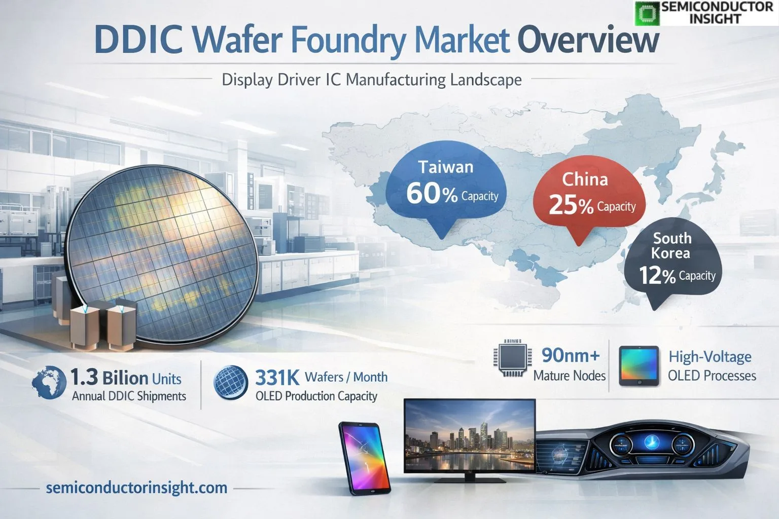
- At the manufacturing level, specialized high-voltage semiconductor processes used for OLED display drivers are projected to reach about 331,000 12-inch wafers per month globally, with roughly 91,000 wafers dedicated to 28/40nm processes used in advanced OLED drivers.
Display Electronics Expanding the Semiconductor Footprint
The scale of modern display manufacturing highlights how essential DDIC wafer fabrication has become. A single high-resolution smartphone display can require multiple driver chips to manage pixel columns and rows, while large televisions or automotive displays may integrate additional timing controllers and interface drivers.
Globally, the semiconductor industry generated about $555 billion in revenue in the past years, according to the Semiconductor Industry Association, with display-related chips representing a notable portion of that ecosystem.
Display panels themselves are produced in enormous volumes. Industry manufacturing reports estimate that hundreds of millions of smartphones and televisions ship annually, creating continuous demand for display driver chips that must be fabricated on silicon wafers before being packaged and integrated into panels. As screen resolutions climb toward 4K and 8K and refresh rates exceed 120Hz, each panel requires more complex driver circuitry, reinforcing the need for specialized foundry capacity.
Asia’s Manufacturing Hubs Dominate DDIC Fabrication
- Semiconductor foundry capacity for display drivers is highly concentrated in Asia. Taiwan, China, and South Korea collectively account for more than 90% of global DDIC wafer production capacity, reflecting the close geographic relationship between chip fabrication plants and display panel manufacturers.
- Taiwan alone holds about 60% of global DDIC foundry capacity, led by companies such as Taiwan Semiconductor Manufacturing Company and United Microelectronics Corporation. These manufacturers operate process nodes optimized for display drivers, particularly 90-150nm technologies, which remain widely used for LCD panels due to their reliability and cost efficiency.
- China has expanded rapidly in recent years, contributing roughly 25% of global wafer starts for display driver chips. Government supported programs between 2021 and 2023 that are directed approximately $21 billion toward semiconductor manufacturing development, helping local foundries scale up capacity and shorten design-to-prototype cycles to nearly 72 hours for some display chip
- South Korea accounts for about 12% of global DDIC manufacturing, focusing largely on high-end OLED driver chips integrated into premium smartphones and televisions.
Mature Process Nodes Still Power Most Display Chips
Unlike high-performance processors that require extremely advanced lithography, many display driver chips are produced using mature semiconductor nodes. Industry analyses indicate that 90nm and larger processes still account for over 70% of DDIC production, particularly for television and mid-range mobile displays.
These process nodes are typically manufactured in 200mm fabs, where wafer lines produce driver chips for large LCD panels. Smaller displays such as smartphones increasingly rely on 300mm fabs using 90nm to 22nm nodes, enabling improved power efficiency and higher data bandwidth for OLED and high-refresh-rate screens.
The coexistence of both mature and advanced nodes makes DDIC manufacturing unique within the semiconductor industry, as foundries must balance legacy wafer equipment with newer high-voltage transistor processes required for modern display panels.
To find out more, feel free to browse our latest updated report: https://semiconductorinsight.com/report/ddic-wafer-foundry-market/
Foundry Specialization and Industry Structure
- The DDIC wafer foundry landscape is shaped by a handful of specialized manufacturing leaders. Taiwan’s foundry ecosystem leads advanced production, with companies developing high-voltage transistor architectures optimized for OLED and LTPO displays. Semiconductor manufacturing disclosures show that some foundries derive a significant portion of their revenue from display driver chips alone.
- For example, one major Asian foundry reported that DDIC manufacturing accounted for roughly 60-70% of its wafer foundry revenue between 2022 and 2025, reflecting the strong dependence of display makers on outsourced chip fabrication.
- Large panel manufacturers also collaborate closely with wafer foundries, allowing rapid iteration of driver designs as display technologies evolve. In some production clusters, panel makers, chip designers, and packaging facilities operate within the same industrial zones, accelerating product development cycles and enabling faster scaling of new display technologies.
Emerging Production Initiatives and Regional Diversification
Although Asia dominates DDIC fabrication today, several countries are attempting to build domestic manufacturing capabilities. In India, a joint venture between HCL Technologies and Foxconn has announced a semiconductor facility designed to process 20,000 wafers per month, representing one of the country’s first initiatives focused on display driver chip production. The project involves an investment of about ₹3,700 crore and is expected to support thousands of semiconductor manufacturing jobs.
Similar initiatives are being explored in other regions as governments seek to reduce reliance on imported semiconductors. However, the technical complexity of display driver fabrication combined with the capital intensity of wafer fabs means that Asia’s existing clusters will likely remain central to the global supply chain for years to come.
In summary, the DDIC wafer foundry market sits at the intersection of semiconductor manufacturing and display technology innovation. As displays continue to evolve toward higher resolution, flexible form factors, and automotive integration, specialized foundry capacity will remain essential for producing the chips that translate digital signals into the vibrant images seen on modern electronic screens.

Comments (0)