
How Semiconductor LPCVD Equipment Market is Powering Advanced Chip Manufacturing?
In semiconductor manufacturing, consistency at the atomic level is not optional it is foundational. Low Pressure Chemical Vapor Deposition (LPCVD) equipment has quietly become one of the most critical tools enabling this precision. Used extensively for depositing silicon nitride, polysilicon, and oxide layers, LPCVD systems operate at pressures typically below 1 Torr and temperatures ranging between 500°C and 900°C. These conditions allow for highly uniform film growth across wafers, which is essential as chip geometries shrink below 10 nm.
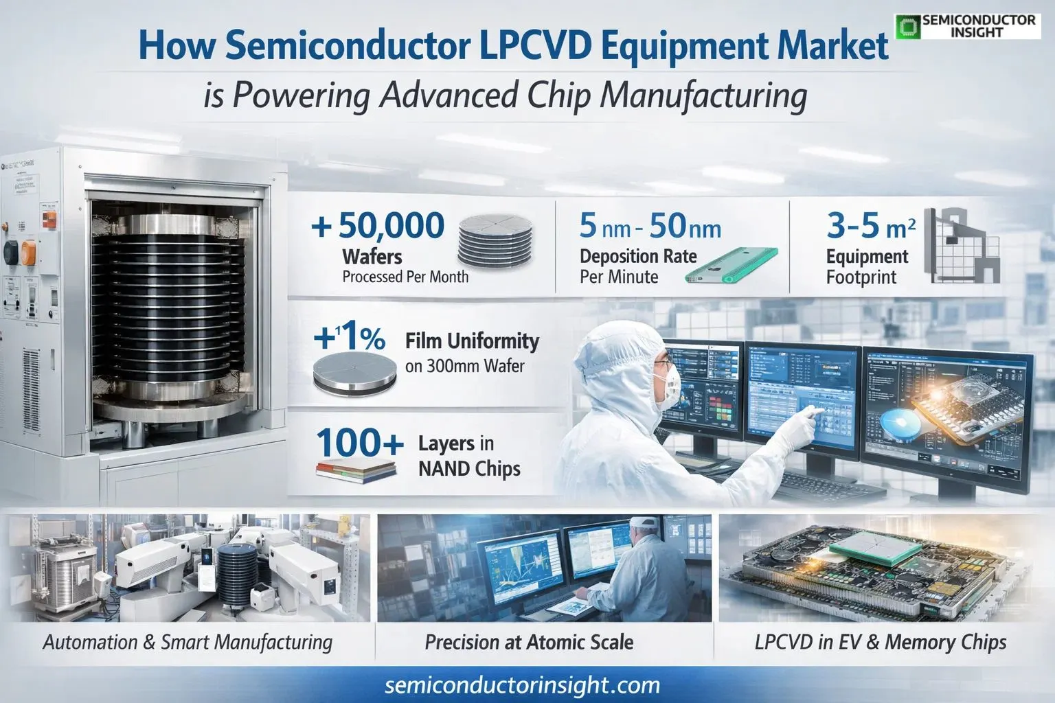
Modern fabrication facilities are now processing more than 50,000 wafers per month in high-volume lines, and a single LPCVD batch furnace can handle between 100 to 150 wafers per cycle. This batch efficiency significantly reduces cost per wafer compared to single-wafer deposition methods, making LPCVD indispensable in large-scale production environments.
Where Numbers Define Performance
- The significance of LPCVD equipment becomes clearer when examining production metrics.
- Film uniformity achieved through LPCVD often falls within ±1% across a 300 mm wafer, a benchmark critical for advanced semiconductor devices.
- Deposition rates typically range from 5 nm to 50 nm per minute depending on the material, allowing engineers to fine-tune processes with remarkable control.
- In memory manufacturing, particularly in DRAM and NAND production, LPCVD systems are used repeatedly across multiple layers.
- A single advanced NAND chip can include over 100 stacked layers, many of which rely on LPCVD-deposited films. This translates into thousands of deposition cycles daily in a single fab, highlighting the scale at which these systems operate.
- Equipment footprint is another defining factor.
- A standard LPCVD furnace system occupies approximately 3 to 5 square meters, yet contributes to processing output valued in millions of dollars per day. This high productivity density is one of the reasons fabs continue investing heavily in upgrading LPCVD capabilities.
The Push toward Advanced Materials
As semiconductor architectures evolve, LPCVD equipment is being adapted to handle increasingly complex materials. Silicon nitride remains a dominant material, accounting for a significant share of LPCVD applications, but there is rising demand for advanced dielectric layers and stress-engineered films.
For example, in logic devices, tensile and compressive stress layers deposited via LPCVD are used to enhance transistor performance. These layers can improve carrier mobility by measurable margins sometimes up to 20% in specific configurations directly impacting chip speed and efficiency.
Additionally, LPCVD is being explored for emerging materials such as silicon carbide (SiC) and gallium nitride (GaN), particularly in power electronics. These materials require higher temperature stability and precise deposition control, pushing equipment manufacturers to refine furnace designs and gas flow dynamics.
Automation and Smart Manufacturing Integration
The integration of LPCVD systems into smart manufacturing ecosystems is reshaping how fabs operate. Modern systems are equipped with real-time sensors that monitor temperature uniformity, gas flow rates, and pressure stability at microsecond intervals. Data collected from these systems can exceed several gigabytes per day per tool, feeding into AI-driven process optimization platforms.
Automation has also significantly reduced human intervention. Today’s LPCVD tools are integrated with robotic wafer handling systems capable of transferring wafers in under 5 seconds per cycle. This not only improves throughput but also minimizes contamination risks, which can otherwise reduce yield by measurable percentages.
Take a Quick Glance at Our In-Depth Analysis Report: https://semiconductorinsight.com/report/semiconductor-lpcvd-equipment-market/
Scaling Challenges and Engineering Responses
- As device dimensions continue to shrink, LPCVD equipment faces new engineering challenges.
- One of the primary concerns is step coverage in high aspect ratio structures, where uniform deposition becomes increasingly difficult.
- Advanced LPCVD systems now incorporate enhanced gas distribution mechanisms to achieve conformality even in structures with aspect ratios exceeding 50:1.
- Another challenge lies in temperature control across larger wafer sizes. With 300 mm wafers being the industry standard, even minor temperature variations can lead to defects.
- To address this, modern furnaces use multi-zone heating systems capable of maintaining temperature variation within ±0.5°C across the chamber.
- Energy consumption is also under scrutiny.
- A single LPCVD furnace can consume between 20 kW to 50 kW during operation. With fabs running dozens of such systems simultaneously, energy optimization has become a priority.
- Newer designs focus on improved insulation and heat recovery systems, reducing overall power consumption by noticeable margins.
Real-World Industry Adoption Snapshots
Leading semiconductor manufacturers are continuously expanding LPCVD capacity to meet rising demand. In recent fab expansions across Asia, new production lines have included over 200 deposition tools, with LPCVD systems forming a substantial portion of this count. These installations are designed to support both logic and memory production, reflecting the versatility of LPCVD technology.
In automotive semiconductor manufacturing, LPCVD plays a crucial role in producing reliable chips for electric vehicles. With EV production volumes crossing 10 million units annually, the demand for high-reliability chips many of which rely on LPCVD processes has surged significantly.
Evolving Design Philosophy in LPCVD Systems
The design of LPCVD equipment is shifting toward modularity and flexibility. Manufacturers are developing systems that can be reconfigured for different processes, reducing downtime and increasing tool utilization rates. Some modern systems now achieve utilization rates above 90%, a significant improvement over older generations.
Additionally, there is a growing emphasis on compact designs without compromising throughput. This allows fabs to maximize cleanroom space, where every square meter can cost thousands of dollars to maintain annually.

Comments (0)