
Semiconductor Inspection Equipment Market Business Value behind Chip Reliability and Yield Optimization
In modern semiconductor manufacturing, a defect smaller than a dust particle can disrupt an entire production cycle worth millions. This reality explains the growing strategic importance of the semiconductor inspection equipment market, which serves as the quality intelligence system of chip fabrication facilities. Rather than functioning as a supporting technology, inspection equipment has become a core production asset that determines yield, performance, and device reliability.
Semiconductor production involves nearly 400-600 manufacturing steps, where even minor contamination or pattern distortion can affect chip functionality. Inspection technologies continuously scan wafers, photomasks, and packaging structures to detect structural inconsistencies at nanoscale levels, ensuring process control and manufacturing precision.
Inspection Intelligence inside Semiconductor Fabrication Ecosystems
The role of inspection equipment extends across the entire semiconductor production lifecycle. These systems detect defects, classify error types, and provide data insights that help engineers refine manufacturing parameters.
- Wafer Surface Monitoring Systems
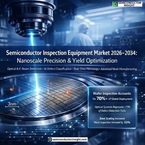
Wafer inspection represents the most significant application area, accounting for more than 70% of inspection equipment deployment globally. These tools detect particle contamination, structural irregularities, and pattern misalignment before further processing stages begin. Early detection prevents expensive rework and enhances manufacturing efficiency.
- Photomask and Reticle Inspection
Photomask inspection ensures accuracy in lithography processes, especially in extreme ultraviolet lithography used for advanced node production. As chip geometries shrink to 3nm and below, inspection tools must detect sub-nanometer defects that could otherwise compromise entire wafer batches.
- Metrology and Measurement Technologies
Metrology equipment measures critical dimensions, overlay alignment, and thickness variations. These measurements ensure circuit patterns match design specifications and maintain electrical performance standards.
Together, these systems enable real-time process monitoring and maintain consistency across high-volume manufacturing environments.
Technology Backbone Driving Detection Precision
- The technological architecture of semiconductor inspection equipment combines multiple detection methods to achieve ultra-high sensitivity.
- Optical inspection systems dominate the market, accounting for nearly 71% of deployed defect detection tools globally due to their speed and scalability. These systems use bright-field and dark-field imaging to identify surface anomalies quickly.
- Electron beam inspection technologies provide higher resolution analysis, allowing detection of extremely small defects in advanced semiconductor nodes. Though slower than optical systems, they offer unmatched accuracy.
- Meanwhile, AI-powered image recognition systems are transforming inspection processes. Over 2,900 inspection units globally now integrate machine learning algorithms for pattern recognition and automated defect classification, significantly reducing human intervention.
- This combination of automation and intelligence is turning inspection equipment into predictive quality management systems rather than simple detection tools.
Business Value and Benefits from Client Perspective
For semiconductor manufacturers and investors, the adoption of inspection equipment delivers measurable operational and financial advantages.
The most significant benefit is yield optimization. Early defect detection prevents defective chips from progressing through production, reducing material waste and operational losses. Even a small yield improvement can translate into millions in additional revenue for high-volume fabrication facilities.
Another major advantage is process stability and reliability. Inspection systems continuously monitor production parameters, ensuring consistent chip performance across batches. This consistency is critical for industries such as automotive electronics, aerospace systems, and medical devices where reliability standards are strict.
Inspection equipment also supports faster innovation cycles. Advanced monitoring allows manufacturers to experiment with new materials and architectures while maintaining process control, accelerating technology commercialization.
Additionally, automated inspection reduces manual quality checks, improving production efficiency and enabling scalable manufacturing environments.
Operational Limitations and Disadvantages for Buyers
Despite strong value creation, semiconductor inspection equipment involves several challenges from a client investment perspective.
The primary concern is high capital expenditure. Advanced inspection tools require significant investment and infrastructure upgrades, making adoption difficult for small and mid-scale fabrication facilities.
Another limitation is technical complexity. Equipment calibration, maintenance, and system integration require specialized expertise, increasing operational costs and workforce training requirements.
Inspection processes can also introduce throughput constraints. High-precision detection methods, particularly electron beam inspection, may slow production speed in high-volume manufacturing environments.
Additionally, managing large volumes of inspection data creates challenges in data interpretation and storage, requiring sophisticated analytics platforms.
For many organizations, balancing inspection accuracy with operational efficiency remains a strategic challenge.
Lastly before we wrap up, don’t forget to look at our most recent exclusive report for in-depth insights:
https://semiconductorinsight.com/report/semiconductor-inspection-equipment-market/
Semiconductor Scaling and Inspection Sensitivity Evolution
As semiconductor nodes shrink, inspection requirements grow exponentially. The transition toward nanoscale manufacturing has introduced new defect types, including pattern collapse, edge roughness, and multi-layer misalignment.
The introduction of 3nm chip manufacturing increased demand for mask inspection tools by over 33%, highlighting the growing sensitivity requirements in advanced fabrication processes.
Similarly, the adoption of heterogeneous integration and advanced packaging technologies requires inspection systems capable of analyzing complex multi-layer structures. These developments are pushing equipment manufacturers toward higher resolution imaging and faster processing capabilities.

Comments (0)