
Semiconductor Inspection Equipment Market Analysis Highlights Defect Detection Innovation
Semiconductor inspection equipment refers to advanced systems used to detect, classify, and analyze defects during wafer fabrication, packaging, and final device testing. These tools enable manufacturers to identify process deviations, contamination, pattern irregularities, and structural flaws before they escalate into yield loss or reliability failures.
As semiconductor architectures move toward smaller geometries, heterogeneous integration, and 3D stacking, inspection equipment has transitioned from a supporting role to a core manufacturing enabler. Modern fabs now treat inspection not as a checkpoint, but as a continuous feedback mechanism embedded across production stages.
Why Inspection Has Become Central to Semiconductor Economics?
The cost of manufacturing advanced semiconductor nodes has increased sharply, making defect prevention more valuable than post-process correction. Even a minor process drift can result in substantial financial losses when scaled across high-volume wafer production.
Inspection equipment helps manufacturers maintain tight process windows by offering early visibility into pattern fidelity and material behavior. This capability directly impacts yield optimization, cycle time reduction, and long-term device reliability, all of which are essential in high-performance computing, automotive electronics, and advanced consumer devices.
Technology Evolution inside Inspection Systems
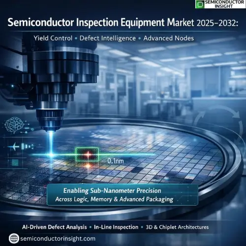
Recent progress in semiconductor inspection equipment is strongly linked to improvements in optical resolution, electron-beam imaging, and data processing algorithms. Optical inspection systems remain essential for high-throughput defect screening, while e-beam tools are increasingly deployed for sub-nanometer defect analysis where optical limits are reached.
Artificial intelligence and machine learning are now integrated into inspection platforms to differentiate between nuisance defects and yield-critical anomalies. This reduces false positives and enables fabs to focus engineering resources on actionable issues rather than manual review.
Another notable development is the shift toward in-line inspection, where tools are embedded directly into the manufacturing flow. This approach supports rapid corrective actions and minimizes material waste.
You Can Go Through Our Latest Updated Insights Here:
https://semiconductorinsight.com/report/semiconductor-inspection-equipment-market/
Inspection across the Semiconductor Manufacturing Lifecycle
Inspection equipment is deployed at multiple stages, each with distinct requirements. Front-end wafer inspection focuses on pattern accuracy, line edge roughness, and particle contamination during lithography and etching processes.
Mid-process inspection plays a crucial role in monitoring layer alignment and material deposition consistency, especially as multi-layer device structures become more complex. Back-end and packaging inspection addresses issues such as bump integrity, interconnect reliability, and bonding accuracy in advanced packaging formats.
The growing adoption of chiplets and 3D integration has further expanded inspection needs beyond traditional wafer surfaces to include interposer layers and vertical interconnections.
Market Demand Drivers and Application Pull
Demand for semiconductor inspection equipment is rising alongside investments in advanced logic, memory, and specialty semiconductor manufacturing. High-growth segments such as artificial intelligence accelerators, electric vehicles, and power electronics require stringent quality standards, reinforcing the importance of inspection precision.
Government-led semiconductor manufacturing initiatives in regions such as Asia-Pacific, North America, and Europe are also contributing to market expansion. New fabs prioritize inspection capability early in facility planning, recognizing its role in accelerating yield ramp-up and stabilizing production.
Competitive Strategies and Industry Positioning
- Leading equipment suppliers are focusing on platform modularity, allowing customers to adapt inspection systems to evolving process nodes without full equipment replacement.
- Software upgrades, enhanced analytics, and compatibility with multiple process steps are becoming standard competitive differentiators.
- Strategic collaboration with foundries and integrated device manufacturers is another key trend.
- Co-development programs enable inspection tool providers to align their roadmaps with next-generation process technologies, ensuring readiness for future manufacturing challenges.
- Smaller, specialized vendors are carving niches by focusing on high-resolution defect review, advanced packaging inspection, or niche materials analysis, complementing broader platform providers.
Operational Challenges and Market Constraints
Despite strong demand, the semiconductor inspection equipment market faces several challenges. High capital costs remain a barrier for smaller fabs and emerging manufacturers, particularly in regions with limited access to funding.
Data complexity is another concern. Advanced inspection systems generate massive volumes of image and process data, requiring robust infrastructure and skilled personnel to extract meaningful insights. Manufacturers are responding by improving software usability and offering integrated analytics solutions.
Supply chain constraints and long equipment lead times can also impact deployment schedules, especially during periods of rapid fab expansion.
At Last, Review the Regional Dynamics and Manufacturing Footprint
- Asia-Pacific continues to dominate inspection equipment demand due to its concentration of semiconductor manufacturing facilities. However, increasing investments in domestic semiconductor production in the United States and Europe are reshaping regional demand patterns.
- These regional shifts are prompting equipment suppliers to expand local support, service networks, and manufacturing capabilities to meet customer expectations for rapid installation and ongoing technical assistance.
Looking ahead, the semiconductor inspection equipment market is expected to grow in both scale and strategic relevance. As device architectures become more complex and tolerance margins narrow, inspection will increasingly serve as a predictive tool rather than a reactive measure.
The convergence of high-resolution imaging, advanced analytics, and real-time process control positions inspection equipment as a foundational pillar of next-generation semiconductor manufacturing. Companies that invest early in inspection capability are likely to achieve faster yield maturity, improved reliability, and stronger competitive positioning.

Comments (0)