
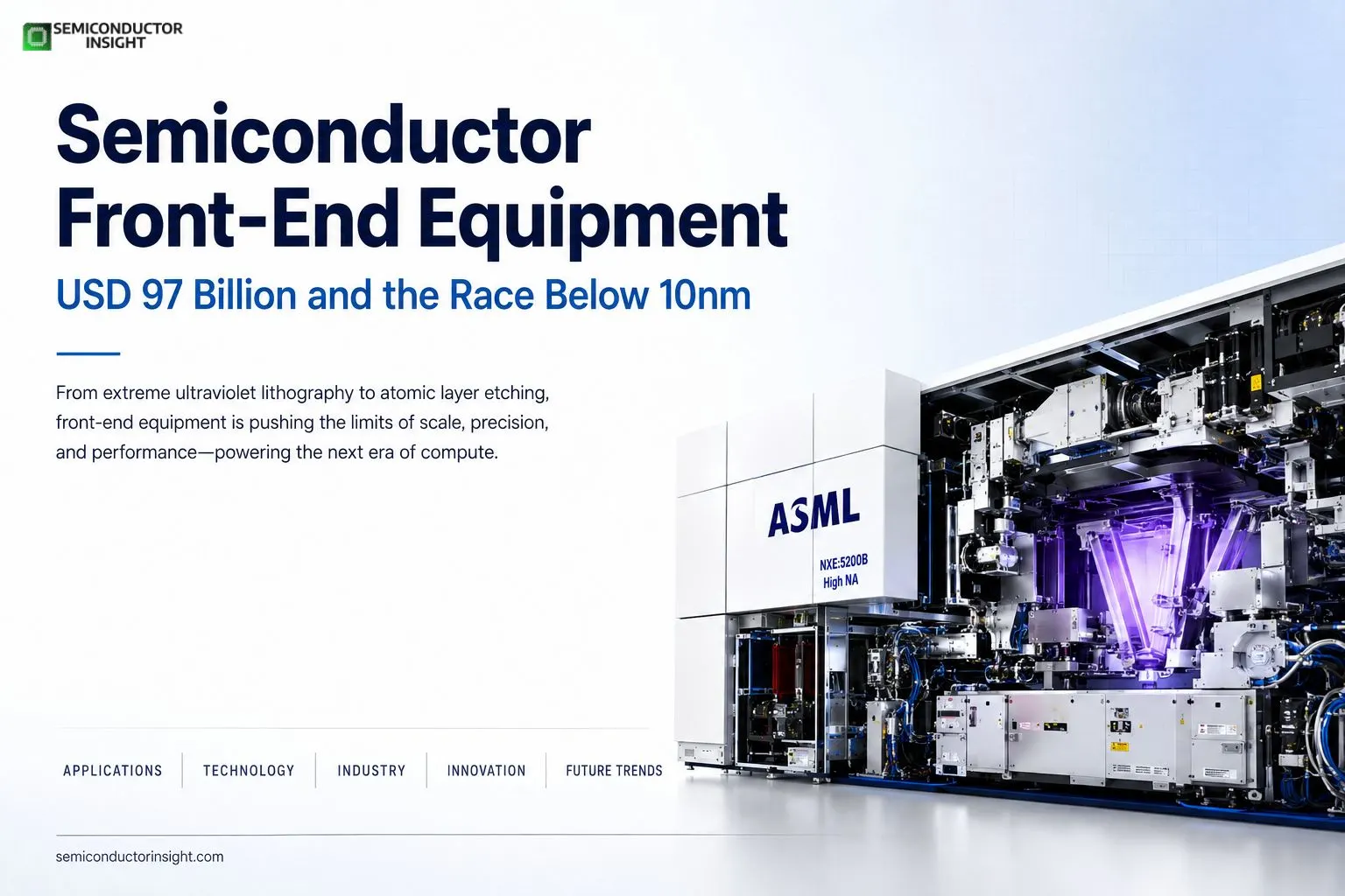
Semiconductor Front-End Equipment Market 2026: USD 97 Billion and the Race Below 10nm
Building a microchip is a manufacturing feat that rivals anything in heavy industry. The front-end of a semiconductor fab-where billions of transistors are carved into silicon wafers-is a world of extreme ultraviolet light, atomic‑layer etching, and nanometer‑scale deposition. The machines that perform these tasks are not off‑the‑shelf tools. They are custom‑engineered giants, each costing millions or even hundreds of millions of dollars, and they are the reason that a single advanced logic fab can now exceed $20 billion in capital investment. In 2026, the global market for semiconductor front‑end equipment is measured in the tens of billions, and its growth is a direct reflection of humanity’s hunger for compute, memory, and connectivity.
Industry data places the market at approximately USD 97.07 billion in 2024, with a projection to reach USD 154.25 billion by 2032-a compound annual growth rate of 7.2 percent. This is not a speculative forecast. It is underpinned by the physical reality that every new smartphone processor, AI accelerator, and high‑bandwidth memory stack requires an increasingly complex set of deposition, patterning, and inspection steps.
Lithography: the engine that pulls everything else
The segmentation of this market tells its own story. Among the major equipment types-etch, deposition, metrology, cleaning, CMP, and lithography-it is the lithography machines that capture both the largest share and the most attention. A single high‑NA extreme ultraviolet scanner from ASML, the Dutch lithography giant, costs north of $300 million and requires a fleet of 747 cargo planes to transport. These tools are the gatekeepers of Moore’s Law. Without them, the sub‑10‑nanometer logic nodes that power NVIDIA’s latest GPUs or Apple’s next‑generation silicon would not exist. In 2026, ASML’s order book for high‑NA EUV tools stretches deep into the next decade, and every major logic and memory manufacturer is vying for a slot.
But lithography is not the only star. Etch and deposition equipment, supplied by companies like Lam Research, Applied Materials, and Tokyo Electron, are just as essential. As device architectures shift from planar transistors to gate‑all‑around nanosheets, the number of etching and deposition steps has exploded. A single advanced logic wafer can pass through deposition and etch chambers hundreds of times before it is complete. This pattern multiplication effect means that even modest increases in wafer starts drive disproportionately larger equipment purchases.
Where the equipment goes: foundry, logic, memory
On the application side, the “Foundry and Logic Equipment” segment dominates. The fabless semiconductor model, where companies like AMD, Qualcomm, and Apple design chips that are manufactured by TSMC, Samsung, and Intel Foundry, concentrates demand into a small number of highly capitalised production hubs. When TSMC places an order for 100 etch chambers, it moves the entire industry. In 2026, the race to 2‑nanometer and sub‑2‑nanometer process nodes is the single largest driver of front‑end equipment spending. Every shrink in transistor size requires more precise, more costly tools.
Memory equipment, serving NAND flash and DRAM manufacturers, is a more cyclical but equally vital segment. The transition to 3D NAND with over 300 layers, and the development of next‑generation DRAM using extreme ultraviolet lithography, is sustaining a parallel investment wave. Memory fabs in South Korea, Japan, and increasingly the United States are absorbing a significant share of deposition and etch tools. The “Others” category, which includes equipment for analog, power, and MEMS devices, contributes a smaller but steady base load of demand, often relying on trailing‑edge nodes that are less capital‑intensive but still require modern 200‑millimeter toolsets.
The sub‑10nm frontier and the technology node split
The market’s segmentation by technology node reveals the premium placed on leading‑edge fabrication. The “<10nm” segment, which encompasses 7nm, 5nm, 3nm, and the emerging 2nm nodes, is where the most expensive equipment is deployed. At these geometries, traditional argon fluoride immersion lithography is augmented or replaced by EUV, and the tolerances for defects shrink to single‑digit parts per billion. Metrology and inspection tools, including electron‑beam and optical wafer inspectors, become critical, as a single undetected particle can kill a die worth hundreds of dollars.
Nodes between 10nm and 20nm, along with the 20–28nm and above‑28nm brackets, still account for a meaningful volume of equipment sales. These nodes serve a vast ecosystem of microcontrollers, power management ICs, image sensors, and RF chips that do not require bleeding‑edge lithography but still demand advanced deposition and etch capabilities. The 28‑nanometer node, in particular, has proven remarkably durable, acting as a cost‑sweet spot for many IoT and automotive applications, and it continues to attract capacity expansions.
Who buys the equipment: IDMs, foundries, memory makers
The end‑user segmentation captures the evolving structure of the semiconductor industry. Integrated Device Manufacturers, or IDMs-companies like Intel, Samsung, and STMicroelectronics that both design and manufacture chips-remain key consumers. However, the balance of power is shifting toward pure‑play foundries like TSMC and GlobalFoundries, which serve hundreds of fabless customers. Foundries now account for a dominant share of leading‑edge capital expenditure, driven by the insatiable demand for advanced logic from AI, cloud, and mobile markets.
Memory manufacturers form a third, highly concentrated buying group. The DRAM market, dominated by Samsung, SK hynix, and Micron, and the NAND market, where Kioxia and Western Digital also play, are investing heavily in equipment to support the transition to next‑generation architectures. The “Others” category includes captive fabs at automotive and industrial companies, as well as research institutions and government‑backed pilot lines.
A 2026 signal: the re‑shoring of fab equipment demand
A tangible development in 2026 is the geographic diversification of equipment purchases. For decades, the vast majority of front‑end equipment was shipped to fabs in Taiwan, South Korea, and China. The CHIPS Act in the United States, the European Chips Act, and similar initiatives in Japan and India are now translating into real construction contracts. In Arizona, TSMC’s fab is ramping production and ordering equipment for a second phase. In Ohio, Intel’s greenfield site is taking shape, with initial tool move‑ins beginning. In Germany, a joint venture between TSMC and European partners is breaking ground. Each of these sites represents a fresh round of demand for the entire equipment supply chain, and the 7.2 percent CAGR through 2032 partly reflects this structural expansion of the global fab footprint.
The semiconductor front‑end equipment market is not a consumer story. It is the story of the tools that make the tools that run the world. The numbers-$97 billion today, heading toward $154 billion-are large enough to matter, but the real drama lies in the precision, the complexity, and the sheer ambition of the engineering required to keep Moore’s Law limping forward for another generation. In 2026, that drama is being written in cleanrooms from Hsinchu to Hillsboro, one atomic layer at a time.
ownload the Full Research Report: https://semiconductorinsight.com/report/semiconductor-front-end-equipment-market/

Comments (0)