
Semiconductor Engineering Powering the Next Phase of LiDAR Market
LiDAR Market is fundamentally a semiconductor story, where precision sensing is enabled by a tightly integrated combination of laser diodes, photodetectors, and signal processing chips. At its core, LiDAR systems rely on semiconductor components to emit laser pulses, detect reflected signals, and convert optical information into digital data that machines can interpret in real time. Unlike traditional optical systems, modern LiDAR solutions are increasingly transitioning toward solid-state architectures, eliminating mechanical parts and relying entirely on chip-level designs for scanning and detection.
This shift is largely driven by advancements in complementary metal-oxide semiconductor (CMOS) fabrication and silicon photonics, allowing LiDAR systems to become smaller, more energy-efficient, and scalable for mass deployment. Semiconductor foundries are now producing specialized chips that integrate laser emission, detection, and processing within compact modules, significantly reducing system complexity and cost. The growing adoption of these integrated solutions reflects a broader movement toward miniaturization and high-volume semiconductor manufacturing.
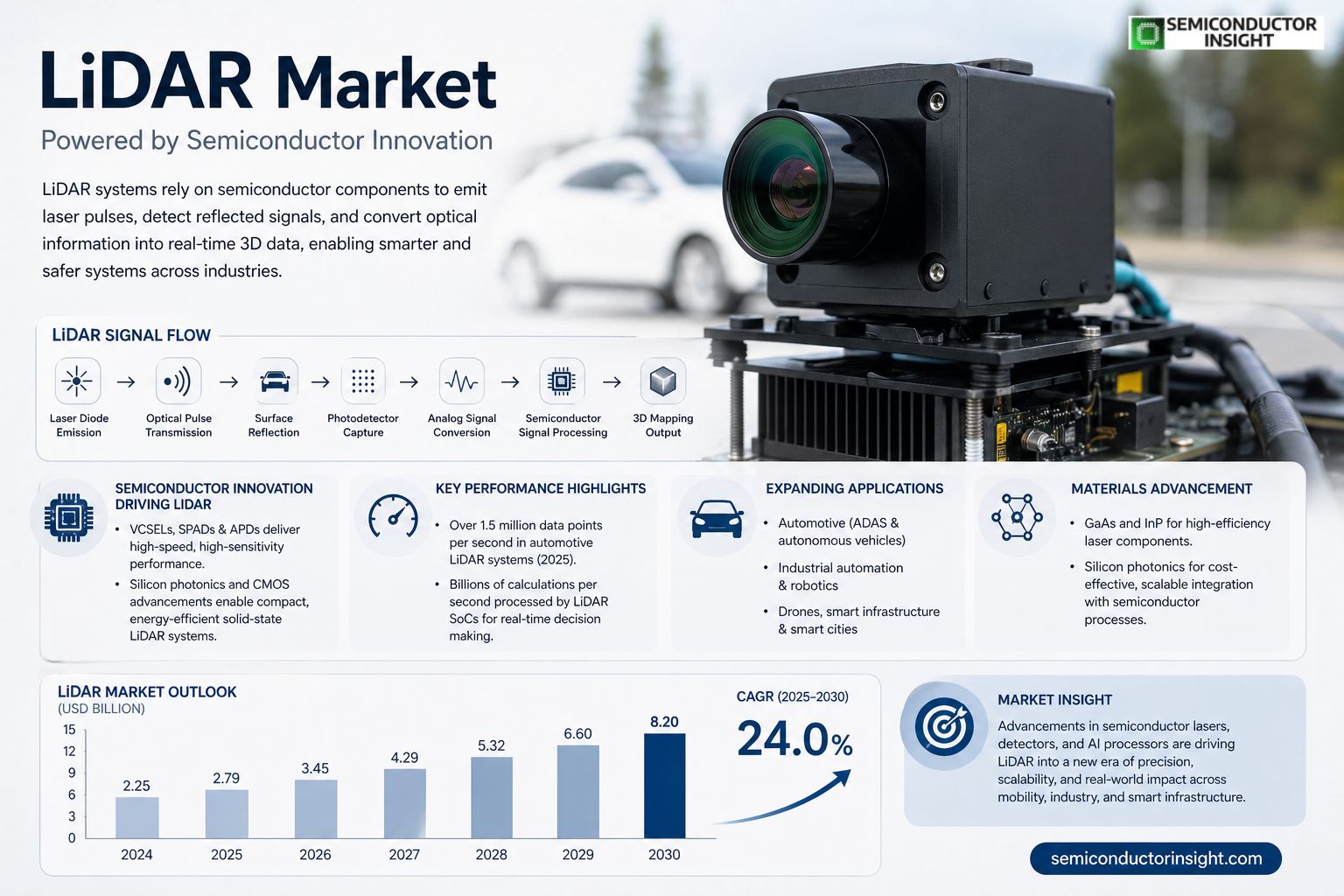
Signal Generation to Data Output Flow in LiDAR Systems
Laser Diode Emission → Optical Pulse Transmission → Surface Reflection → Photodetector Capture → Analog Signal Conversion → Semiconductor Signal Processing → 3D Mapping Output
Chip Level Innovation in Laser and Detector Technologies
The performance of LiDAR systems depends heavily on the efficiency of semiconductor lasers and photodetectors. Vertical-cavity surface-emitting lasers (VCSELs) and edge-emitting lasers are widely used due to their ability to produce consistent and high-frequency pulses. On the detection side, avalanche photodiodes (APDs) and single-photon avalanche diodes (SPADs) have become critical components, offering high sensitivity even in low-light conditions.
Recent semiconductor advancements have enabled SPAD arrays to operate at extremely high speeds, processing millions of photons per second. This is particularly important in automotive LiDAR systems, where real-time decision-making depends on rapid data acquisition. In 2025, semiconductor-based LiDAR sensors used in advanced driver-assistance systems (ADAS) were capable of generating over 1.5 million data points per second, enabling highly detailed environmental mapping.
Fabrication Complexity and Wafer Scale Integration
- LiDAR semiconductor manufacturing involves complex processes that combine traditional silicon wafer fabrication with advanced photonic integration.
- Foundries are increasingly adopting hybrid manufacturing techniques where optical components are embedded directly onto silicon substrates.
- This approach enhances signal efficiency while reducing power consumption.
- Global semiconductor production exceeded over 1 trillion chips annually, and a growing fraction of these are dedicated to sensing and photonics applications, including LiDAR.
- The transition toward wafer-scale integration allows manufacturers to produce LiDAR chips in higher volumes, supporting applications beyond automotive, such as drones, industrial automation, and smart infrastructure.
- Thermal management is another critical factor in chip design.
- High-performance LiDAR systems generate significant heat due to continuous laser operation, requiring advanced semiconductor materials and packaging solutions to maintain stability and performance.
Data Processing Power and AI Integration at Chip Level
Beyond sensing, LiDAR systems rely heavily on semiconductor processors to convert raw data into actionable insights. Application-specific integrated circuits (ASICs) and system-on-chip (SoC) designs are increasingly used to handle complex algorithms, including object detection and real-time mapping.
Modern LiDAR processors can handle billions of calculations per second, enabling features such as obstacle detection, lane recognition, and environment reconstruction. This integration of sensing and processing within semiconductor architectures is a key factor driving the scalability of LiDAR technology.
In autonomous vehicles, for instance, LiDAR data is combined with inputs from cameras and radar, all processed through semiconductor-based AI chips. This multi-sensor fusion enhances accuracy and reliability, making LiDAR an essential component of next-generation mobility systems.
Take a Quick Glance at Our In-Depth Analysis Related Report: https://semiconductorinsight.com/report/global-lidar-services-market/
Expanding Semiconductor Demand across End Use Applications
- LiDAR Market is expanding rapidly across multiple sectors, each placing unique demands on semiconductor components.
- In automotive applications, LiDAR is becoming a critical element of safety systems, with several vehicle manufacturers integrating it into production models.
- By 2026, autonomous and semi-autonomous vehicles are expected to account for a significant share of LiDAR chip demand.
- In industrial automation, LiDAR systems are used for precision mapping and navigation in warehouses and manufacturing plants.
- Robotics applications, including autonomous drones, rely on compact semiconductor-based LiDAR modules for navigation and obstacle avoidance.
- Smart city infrastructure is another emerging area, where LiDAR sensors are deployed for traffic monitoring, urban planning, and environmental analysis.
- Governments and municipalities are increasingly investing in such technologies, further driving semiconductor demand.
Semiconductor Material Evolution and Performance Enhancement
Material innovation is playing a crucial role in improving LiDAR performance. Gallium arsenide (GaAs) and indium phosphide (InP) are widely used in laser components due to their superior optical properties compared to silicon. These compound semiconductors enable higher efficiency and longer-range detection, which are essential for applications like autonomous driving.
At the same time, silicon photonics is gaining traction as a cost-effective alternative, allowing optical components to be integrated with traditional semiconductor processes. This combination of materials is enabling the development of hybrid systems that balance performance and scalability.

Comments (0)