
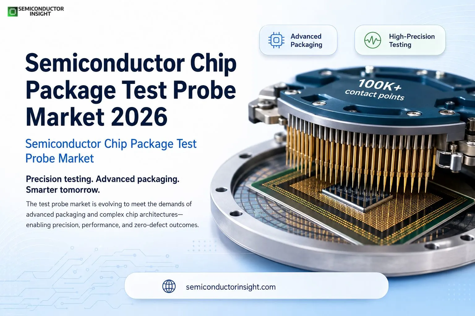
Semiconductor Chip Package Test Probe Market 2026: Why Advanced Packaging Innovators Are Paying Attention?
The semiconductor chip package test probe sector stands at a pivotal intersection of precision engineering and explosive demand for reliable high-performance electronics. As chips grow more complex with heterogeneous integration and 3D stacking, the tools that verify their packaged integrity after assembly have become indispensable.
This space is experiencing steady expansion fuelled by the need for accurate electrical contact at finer pitches and higher frequencies.
Navigating the Precision Demands of Modern Packaged Devices
- Engineers working on next-generation systems face unique hurdles when testing packaged chips.
- Traditional probe technologies struggle with the dense interconnects in fan-out wafer-level packaging or embedded bridge solutions.
- Vertical MEMS-style probes and advanced cantilever designs now deliver the compliance and low contact resistance needed to maintain signal integrity without damaging delicate bumps or pillars.
- Real-world implementations highlight this shift. Intel’s Embedded Multi-Die Interconnect Bridge (EMIB) technology, used in high-end AI accelerators, requires probing solutions capable of handling multi-die configurations where power delivery and thermal management add layers of complexity.
- Similar demands appear in TSMC’s CoWoS platforms, where test probes must verify thousands of high-bandwidth connections post-packaging. These examples show how probe technology directly influences yield and time-to-market for cutting-edge processors.
To Know More about the Report, You Can Freely Browse Our Latest Updated Report: https://semiconductorinsight.com/report/semiconductor-chip-package-test-probe-market/
Evolving Probe Architectures for High-Frequency and High-Power Applications
Probe designs have advanced significantly to support RF and power-hungry devices. Palladium alloy foil probes offer improved durability and consistent electrical performance across temperature variations, making them suitable for automotive-grade and data centre components. IEEE technical discussions emphasise the move toward arrays supporting over 100,000 contact points per card, enabling full-wafer or package-level validation in a single touchdown.
In practice, manufacturers integrate thermal stabilisation techniques during probing to minimise drift in high-current tests. One approach uses heat-conductive wafers for soaking probe cards, reducing setup times and improving repeatability across production runs. This matters immensely for silicon photonics and wide-bandgap devices entering mainstream production.
Government Initiatives Reshaping Domestic Testing Capabilities
- Policy moves like the U.S. CHIPS and Science Act have directed resources toward strengthening the entire semiconductor ecosystem, including advanced packaging and associated test infrastructure.
- The National Advanced Packaging Manufacturing Program supports shared research facilities where companies can prototype and validate new probing methods alongside novel substrates and interconnects. This investment aims to reduce reliance on concentrated overseas supply chains while accelerating innovation in domestic facilities.
- Projects in Arizona and other hubs demonstrate practical outcomes, with facilities incorporating testing lines that handle both front-end wafer probing and post-packaging validation.
- These developments create opportunities for closer collaboration between foundries, OSAT providers, and probe specialists, shortening development cycles for AI and high-performance computing applications.
Material Innovations Driving Probe Longevity and Performance
Material science breakthroughs play a central role in extending probe life under demanding conditions. Studies on palladium-copper-silver alloys reveal near-isotropic mechanical properties, allowing reliable operation regardless of probe orientation. This uniformity reduces variability in high-volume manufacturing environments where millions of touchdowns occur daily.
Additional focus areas include low-inductance designs for power integrity and coatings that minimise scrub marks on sensitive package surfaces. Such refinements help maintain device reliability, especially in applications like 5G infrastructure and electric vehicle power modules, where failure rates must stay exceptionally low.
Integration with System-Level Testing Workflows
Modern test flows increasingly blend package-level probing with system-level validation. Adaptive testing strategies use real-time data to adjust parameters, optimising coverage while controlling costs. Probe stations now incorporate software ecosystems for automated alignment and recipe management, cutting engineering debug time substantially.
Case examples from sensor manufacturers show custom probe setups boosting throughput for specialised devices. These integrations prove especially valuable when dealing with chiplet-based architectures, where individual dies and their interconnections must all pass rigorous checks before final assembly.
Global Supply Chain Dynamics and Technology Diffusion
Geopolitical factors and capacity expansions influence how probe technologies spread. New fabrication investments in multiple regions create parallel demand for compatible testing solutions. Companies explore hybrid approaches that combine established cantilever methods with emerging MEMS vertical arrays to balance cost and capability.
Ongoing work in heterogeneous integration highlights the need for probes that accommodate mixed-node chiplets. Standards development through industry bodies helps align requirements across the supply chain, facilitating smoother adoption of advanced packaging formats worldwide.
Emerging Opportunities at the Edge of Innovation
- The continued push toward tighter pitches below 40 micrometres and support for higher current densities open avenues for specialised probe solutions in photonics and quantum-adjacent technologies.
- Early adopters in research consortia experiment with non-contact or wireless concepts, though mechanical probing remains dominant for production environments.
As AI workloads scale and automotive electrification accelerates, the semiconductor chip package test probe domain will keep evolving. Success depends on close alignment between material scientists, equipment designers, and end users who demand zero-defect outcomes in increasingly sophisticated packages. The coming years promise further refinement of these critical interfaces that ensure tomorrow’s chips perform reliably from the first power-on.

Comments (0)