Samsung Taps Korean Partners to Advance Low-Temp ALD Precursors for GAA Chips
In the race to power the next generation of electronic devices, the semiconductor industry is pushing technological boundaries at unprecedented speeds. Among the unsung heroes of this transformation are silicon precursors used in atomic layer deposition (ALD) and chemical vapor deposition (CVD) processes. These chemical compounds form the bedrock of advanced material deposition, enabling extreme miniaturization, improved performance, and enhanced energy efficiency in microchips.
According to recent data, the global semiconductor ALD and CVD silicon precursors market was valued at US$ 1.23 billion in 2024 and is projected to reach US$ 2.08 billion by 2032, expanding at a CAGR of 7.8% between 2025 and 2032. This robust growth trajectory underscores how pivotal these materials are in advancing chip design, particularly as manufacturers move toward 2nm and even sub-angstrom technologies.
Access Your Free Sample Report- Semiconductor ALD and CVD Silicon Precursors Market
- Intel and TSMC: Material Engineering for Angstrom-Era Nodes
Industry giants Intel and TSMC are spearheading a new wave of innovation by reimagining silicon precursor chemistry. As both companies target 2nm and Angstrom-class nodes, the need for highly controlled deposition processes has become critical.
Intel is working closely with material suppliers to develop engineered organosilicon compounds that enhance film conformality in 3D architectures like FinFET and gate-all-around (GAA) transistors. These advanced silicon precursors feature precise atomic layering capabilities, enabling the formation of uniform dielectric and conductive films even on high-aspect-ratio structures.
Similarly, TSMC is investing in bespoke precursor design in collaboration with Air Liquide and JSR Corporation. Their goal? Lower thermal budgets and minimize defectivity during the deposition process. This is especially vital for logic chips that operate at high frequency and low voltage, where thermal sensitivity is paramount.
Key Takeaway: Custom-designed precursors tuned for low-temperature, high-uniformity deposition are becoming a strategic differentiator in high-end chip manufacturing.
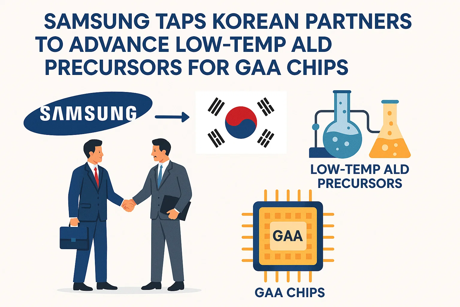
- Samsung’s Drive Toward GAA Leadership
Samsung Electronics is doubling down on its transition to Gate-All-Around (GAA) transistors—a shift that demands new classes of silicon precursors. With the GAA structure’s emphasis on precise nanowire channel wrapping, even atomic-scale inconsistencies in film growth can compromise performance.
To meet these challenges, Samsung is partnering with domestic innovators such as DNF Co. and SK Materials. The collaboration focuses on low-temperature ALD silicon precursors that can form ultra-thin, high-k dielectric layers with excellent uniformity and minimal edge roughness.
Samsung’s approach reflects a broader industry trend: integrating materials science into device design to achieve power, performance, and area (PPA) goals. By focusing on precursor reactivity and decomposition profiles, Samsung aims to ensure more consistent growth rates and improved electrical properties.
Key Takeaway: In the age of GAA, the focus is not just on device architecture but also on the atomic-level interactions that underpin material deposition.
- Air Liquide’s Billion-Dollar Bet on Asia
Air Liquide, a global leader in industrial gases and advanced materials, has committed $1.2 billion to expanding its gas production capabilities in Taiwan and South Korea. The investment is heavily focused on semiconductor-grade silicon and metal precursors, directly addressing the surging demand from chip fabs.
This expansion involves establishing on-site synthesis and purification facilities, allowing Air Liquide to deliver ultra-high-purity precursors tailored to each fab’s specifications. This model reduces the logistical and contamination risks associated with transporting volatile chemicals over long distances.
Notably, Air Liquide’s push reflects a growing demand for just-in-time precursor delivery with purity levels exceeding 99.9999999% (9N). As chip geometries shrink, even trace impurities can lead to catastrophic failures, making ultra-pure precursor management a competitive necessity.
Key Takeaway: Proximity to fabs and ultra-pure precursor delivery systems are emerging as critical factors in supplier selection.
Download Sample Report PDF- Semiconductor ALD and CVD Silicon Precursors Market
- Entegris and Merck’s EUV-Ready Silicon Precursors
As EUV (Extreme Ultraviolet Lithography) becomes mainstream for advanced nodes, supporting materials like silicon precursors must adapt to new requirements. Entegris and Merck KGaA (formerly Versum Materials) are leading this transition by engineering EUV-compatible silicon precursors.
These precursors are tailored for PEALD (Plasma-Enhanced ALD) processes, offering high volatility and low residue formation. The aim is to support EUV hardmask applications and spacer patterning, where cleanliness and precision are paramount. By minimizing the inclusion of nitrogen and carbon contaminants, these precursors also reduce post-deposition defects.
Entegris, in particular, has developed novel precursor containers and delivery modules to handle these sensitive chemicals more safely and efficiently. The company’s integrated approach—combining materials and delivery technology—offers an edge in reducing downtime and enhancing process yield.
Key Takeaway: Compatibility with EUV lithography and integrated delivery systems is reshaping precursor development strategies.
- Regulatory Winds: The Move Toward PFAS-Free Chemistry
In response to increasing regulatory scrutiny, the industry is pivoting toward PFAS-free silicon precursors. PFAS (per- and polyfluoroalkyl substances), often referred to as “forever chemicals,” are under global review due to their environmental persistence and health risks.
Leading players like Linde, Matheson, and Lam Research are trialing PFAS-free alternatives that maintain performance while adhering to upcoming EU and U.S. EPA restrictions. These efforts are not just regulatory compliance measures—they’re part of a broader sustainability movement within the semiconductor sector.
Beyond regulation, going PFAS-free also reduces the burden of waste treatment and chemical recycling, aligning with the carbon neutrality goals of major chipmakers.
Key Takeaway: Environmental compliance is not just a checkbox—it’s a driver of chemical innovation and supply chain reconfiguration.
- Equipment Makers Step Up: AI and Automation in Precursor Delivery
Equipment giants like Tokyo Electron (TEL) and Applied Materials are innovating beyond traditional tool design. Their focus? Leveraging AI-driven precursor flow control systems to optimize film uniformity and minimize chemical waste.
Tokyo Electron’s recent tools include software-controlled real-time monitoring of precursor decomposition and deposition rates. This feedback system ensures more consistent film characteristics, even in complex 3D structures.
Meanwhile, Applied Materials has unveiled next-generation precursor delivery modules that improve the handling of volatile and reactive silicon precursors. These systems emphasize leak-tight seals, advanced vaporizer technologies, and modular refill cartridges, offering fabs improved safety and operational uptime.
Key Takeaway: Smart tools that combine chemistry and software are setting new standards in deposition process control.
Click Here To Download Full Sample Report- Semiconductor ALD and CVD Silicon Precursors Market
The Road Ahead
The future of semiconductors lies not only in design innovation but also in the materials that make those designs possible. ALD and CVD silicon precursors, once seen as commoditized chemicals, are now central to solving the industry’s most pressing challenges—from high aspect ratio fill to EUV compatibility, PFAS elimination, and AI-enhanced process control.
As the market marches toward US$ 2.08 billion by 2032, the silicon precursor ecosystem will be shaped by tight partnerships between device makers, material suppliers, equipment OEMs, and regulators. The goal is clear: atomic-scale precision, zero-defect reliability, and environmentally responsible manufacturing.
In this high-stakes race, the companies that master the intersection of material science, regulatory foresight, and smart automation will define the semiconductor landscape for years to come.
Further Reading:
- Reuters: “Intel’s Material Playbook for Angstrom-Era Chips”
- Nikkei Asia: “TSMC Strengthens Supply Chain for 2nm”
- Business Korea: “Samsung and DNF Co. to Develop GAA-Compatible Precursors”
- Financial Times: “Air Liquide’s Asia Strategy: Fabs, Gas, and Growth”
- EE Times: “Entegris Develops EUV-Ready Silicon Precursors”
- NYT & Nature News: “PFAS Regulations and the Semiconductor Industry”
Comments (0)