

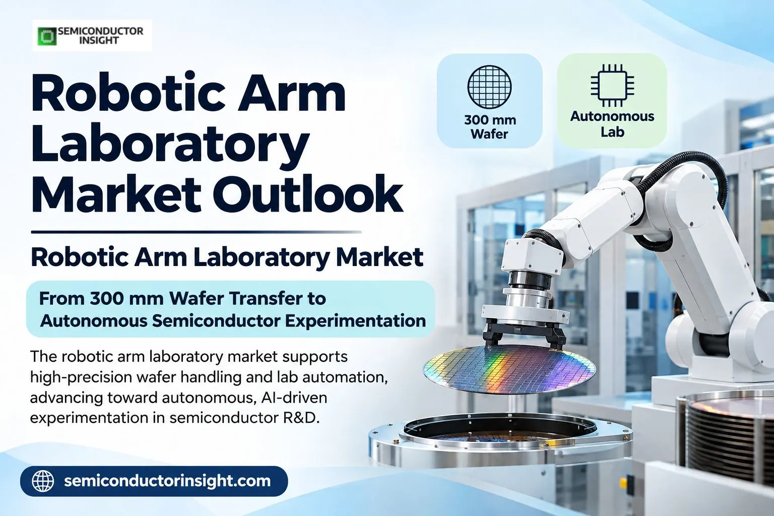
Robotic Arm Laboratory Market Outlook: From 300 mm Wafer Transfer to Autonomous Semiconductor Experimentation
Robotic Arm Laboratory Market is developing around a new requirement in semiconductor engineering: performing delicate research and material-handling operations with repeatable accuracy, controlled movement and minimal contamination. These systems are used in semiconductor research laboratories, wafer-processing environments, metrology facilities, and microelectronics testing centres and advanced-materials experiments. Their capabilities range from transferring silicon wafers between process chambers to positioning optical components and handling sensitive laboratory equipment.
In 2026, the market is moving beyond conventional pick-and-place automation. Machine vision, vacuum-compatible mechanisms, collaborative manipulation and AI-based control are changing how laboratories design experiments and manage high-precision workflows.
When a Wafer Transfer Becomes a Precision Engineering Task
- Semiconductor laboratories require robotic arms that can move wafers without introducing particles, scratches or positioning errors. This is particularly important in advanced lithography and inspection environments, where a small handling inconsistency can affect subsequent measurements or processing stages.
- ASML’s EUV technology illustrates the precision involved. Its published technical explanation describes wafer-handler robot arms that transfer wafers through an airlock into and out of a vacuum environment, with positioning accuracy of 25 micrometres.
- The wafer stage itself operates at a much finer level, positioning the wafer to within a quarter of a nanometre and checking and adjusting its position 20,000 times per second.
- These specifications demonstrate why laboratory robotics must be designed around the entire process environment rather than simply the movement of an object.
The 300 mm Wafer Format Is Influencing Robot Architecture
The growing importance of 300 mm wafer processing is shaping the design of front-end automation systems. Hirata Corporation’s semiconductor equipment portfolio includes atmospheric and vacuum wafer-transfer robots, load ports, aligners and Equipment Front End Modules (EFEMs). Its 300 mm EFEM configurations include 2-port, 4-port and 2×2-port arrangements, allowing equipment manufacturers to configure wafer movement around different process-tool layouts.
These systems are also relevant to fan-out panel-level packaging, where robotic handling must accommodate larger panels and different transfer requirements. The expansion of advanced packaging and heterogeneous integration makes flexible material-handling architecture increasingly important for research facilities evaluating new process sequences.
Autonomous Experiments Are Moving Beyond the Laboratory Demonstration
A significant 2026 development came from MIT, where researchers demonstrated a reconfigurable robotic optics laboratory capable of assembling and adjusting experimental equipment. The system uses a robotic arm with seven movable joints to position mirrors, lenses and other optical components. QR-coded component housings help the robot identify individual parts, while cameras and software coordinate positioning, collision avoidance and alignment.
The system demonstrated automated laser-cavity assembly, beam centring, beam alignment and stabilisation. This is relevant to semiconductor research because optical experiments support the development of displays, sensors, solar technologies and other advanced materials. Automating repeated experimental arrangements could reduce the time researchers spend rebuilding and manually adjusting test setups.
You can freely browse our most recent related updated report to learn more about it before scrolling further: https://semiconductorinsight.com/report/robotics-embedded-systems-market/
Physical AI Is Giving Research Arms a New Purpose
- Robotic arms are increasingly being developed as platforms for testing intelligent physical interaction, not simply programmed industrial movements. At SEMICON India 2026, Addverb introduced its JEN 6 QDD robotic arm for Physical AI research.
- Its intended applications include object recognition, grasping, computer vision, reinforcement learning and Vision-Language-Action models. The platform supports wrist-mounted vision systems and a software development kit for data collection and independent arm control.
- For semiconductor laboratories, this development is relevant to research involving electronic-component handling, precision manipulation and AI-assisted automation.
- It also connects robotics research with the semiconductor supply chain itself, where sensors, processors, power electronics and control systems determine how effectively a robot can perceive and respond to its environment.
Cleanroom Automation Is Becoming a Measurable Investment Priority
The broader industrial robotics landscape provides useful context for laboratory equipment demand. According to the International Federation of Robotics, factories worldwide installed 603,000 industrial robots in 2025, while the global operational stock reached approximately 5.079 million units. Electronics installations increased by 10% during the year. India installed almost 10,500 industrial robots, an increase of 15% compared with 2024.
These figures do not represent laboratory-arm installations specifically, but they indicate the wider automation environment in which semiconductor research and manufacturing operate. As laboratories handle increasingly sensitive materials and more complex process equipment, robot selection will depend on cleanroom compatibility, repeatability, payload, reach, vacuum operation and integration with laboratory software.
The Laboratory Is Becoming Part of the Semiconductor Development System
The next stage of Robotic Arm Laboratory Market will be shaped by the connection between physical equipment and intelligent experimental control. Wafer-transfer robots, optical manipulation arms, automated inspection systems and AI-enabled research platforms serve different functions, but they are increasingly linked by the same requirement: reliable, traceable and repeatable operations.
For semiconductor developers, the value of laboratory robotics lies in making experiments easier to reproduce, reducing unnecessary manual handling and supporting more complex research workflows. As advanced packaging, high-precision metrology and AI-assisted materials discovery expand, robotic arms are becoming an important part of the infrastructure used to develop and validate the next generation of semiconductor technologies

Comments (0)