

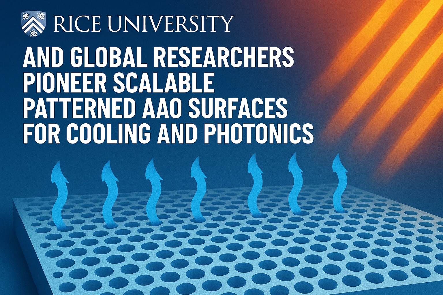
Rice University and Global Researchers Pioneer Scalable Patterned AAO Surfaces for Cooling and Photonics
Anodic Aluminum Oxide (AAO) wafers, also known as anodized aluminum oxide membranes, are rapidly gaining attention across industries ranging from microelectronics to photonics, biosensing, energy storage, and nanotechnology. What makes AAO unique is its highly ordered, self-assembled nanoporous structure, formed through the electrochemical anodization of aluminum. This nanoscale uniformity offers an ideal template for nanowire growth, photonic crystals, membranes, and advanced coatings.
Until recently, AAO wafers were largely confined to research labs and niche applications. However, new manufacturing breakthroughs, industry collaborations, and sustainability trends are pushing AAO into the commercial spotlight. The market trajectory reflects this momentum: the global Anodic Aluminum Oxide Wafer Market was valued at USD 139 million in 2024 and is projected to reach USD 2,746 million by 2032, expanding at a stunning CAGR of 57.7% during the forecast period.
Access Your Free Sample Report- Anodic Aluminum Oxide (AAO) Wafer Market
Understanding the Basics of Anodic Aluminum Oxide (AAO)
Before diving into developments, it’s worth briefly revisiting what AAO wafers are and why they are so significant:
- Formation Process
- AAO is created by anodizing aluminum in acidic electrolytes under controlled voltage and current conditions.
- The process produces a porous oxide layer with hexagonally arranged nanopores, whose size, density, and uniformity can be tuned by adjusting the anodization parameters.
- Key Properties
- Nanopore uniformity: Pore diameters can be finely controlled (10–400 nm range).
- Thermal and chemical stability: AAO films are stable under high temperatures and chemically resistant.
- High surface area: Beneficial for sensors, catalysis, and energy storage.
- Transparency to light and tunable optical behavior: Useful for photonics and optical devices.
- Applications
- Nanotemplate for nanowire growth (semiconductors, metals, polymers).
- Membranes for filtration, water purification, and gas separation.
- Biosensing and diagnostics
- Energy storage (batteries, supercapacitors).
- Photonic and optoelectronic applications.
Recent Developments in the AAO Wafer Industry
1. Breakthrough Patterning Techniques for Enhanced Surfaces
One of the most exciting developments came from a collaborative research effort led by Rice University and the University of Edinburgh. The team developed a scalable method to produce topography-patterned aluminum surfaces through a combination of masking, anodization, and chemical treatment.
- Key outcome: These patterned AAO surfaces demonstrated improved wetting, cooling efficiency, and droplet shedding.
- Industrial relevance: Such surfaces could dramatically enhance electronics cooling, anti-icing in aerospace, and fluid transport in medical devices.
- Why it matters: Traditional AAO fabrication methods often face scalability issues. This breakthrough emphasizes manufacturability, moving beyond laboratory curiosities toward industrial adoption.
This development signals a critical trend: AAO is no longer confined to controlled lab settings but is being engineered with scale and industrial usability in mind.
2. Recycling Aluminum for Sustainable AAO Production
Sustainability is an urgent theme across all advanced materials, and AAO is no exception. A 2024 study highlighted by Light Metal Age demonstrated that recycled aluminum can anodize with results nearly identical to primary (virgin) aluminum when process parameters are carefully controlled.
- Why it’s important: Historically, impurities in recycled aluminum were thought to degrade anodizing quality, leading to pore irregularities.
- New insight: Microstructure, process conditions, and heat treatment may play a larger role than trace impurities in determining anodizing quality.
- Implication: With recycled aluminum proving viable, AAO production could become significantly greener and more cost-effective.
This is especially impactful in Europe and Asia, where circular economy regulations are pressuring manufacturers to adopt recycled inputs. It positions AAO as a sustainable nanomaterial platform in line with global ESG priorities.
3. Carbon-Coated AAO for Enhanced Stability
Another promising development involves carbon-coated anodic aluminum oxide. Researchers have reported new synthesis routes to deposit carbon layers inside AAO pores, enhancing its chemical stability, conductivity, and surface functionality.
- Potential applications:
- Advanced electrodes for lithium-ion and next-gen batteries.
- High-performance catalysts.
- Corrosion-resistant coatings.
- Industry benefit: Carbon functionalization expands AAO’s utility beyond insulating oxide membranes, making it a versatile platform for hybrid materials.
This type of surface engineering underlines how functionalization is the key to unlocking new AAO use cases.
Download Sample Report PDF- Anodic Aluminum Oxide (AAO) Wafer Market
4. Nanopore Geometry Control and Membrane Engineering
AAO’s value lies in its nanoscale pores but achieving consistent pore geometry at scale has been challenging. Recent academic and industrial advances highlight improved methods for:
- Dual-step anodization for superior pore order.
- Novel electrolytes that enable finer pore diameters.
- Graded pore structures that offer multifunctionality (e.g., gradient filtration membranes).
- Defect reduction methods that improve wafer uniformity.
These improvements pave the way for AAO membranes in water purification, biosensing, and even semiconductor manufacturing.
5. Industry Collaboration and Knowledge Sharing
The 2025 Aluminum Summit, which unites anodizers and extruders, emphasizes the growing importance of collaboration in surface finishing and anodizing technologies. For AAO in particular, such forums help:
- Standardize alloy and anodizing practices.
- Share advancements in scalable AAO manufacturing.
- Build bridges between academia, material suppliers, and device manufacturers.
This collaborative spirit is vital because AAO wafer adoption depends on cross-industry alignment from aluminum suppliers to electronics OEMs.
Market Insights and Outlook
Market Size and Growth
- 2024 valuation: USD 139 million.
- 2032 projection: USD 2,746 million.
- CAGR: 57.7% (2024–2032).
Such a steep growth rate suggests AAO wafers are transitioning from experimental materials into commercially viable platforms. The growth is being fueled by:
- Rising demand for nanostructured templates in semiconductors and photonics.
- Increased use in biosensing and healthcare diagnostics.
- Sustainability pressures accelerating recycled aluminum adoption.
- Functionalization advances (carbon-coating, hybrid materials).
- Growing awareness among electronics and materials engineers of AAO’s versatility.
Regional Analysis
- Asia-Pacific (APAC)
- Likely to dominate due to semiconductor manufacturing hubs in China, Taiwan, Japan, and South Korea.
- Strong adoption in water filtration and membranes, particularly in industrial sectors.
- North America
- Growth driven by academic research commercialization (e.g., Rice University breakthrough).
- Applications in electronics cooling, aerospace, and defense.
- Europe
- Strong emphasis on sustainability and recycled aluminum usage.
- Adoption in photonic devices and biomedical research.
Application Outlook
- Electronics & Semiconductors: Templates for nanowire transistors, memory devices, cooling solutions.
- Healthcare & Life Sciences: Biosensors, DNA sequencing platforms, drug delivery.
- Water & Environmental: Membranes for water purification, gas separation.
- Energy Storage: Electrodes for lithium-ion, solid-state batteries, and supercapacitors.
- Photonics & Optoelectronics: Photonic crystals, light management in solar cells.
Challenges Facing the AAO Wafer Industry
Despite the promising outlook, several challenges remain:
- Scalability & Cost
- Producing defect-free AAO wafers at wafer-scale dimensions is still costly.
- Process optimization is needed to reduce waste and energy consumption.
- Uniformity & Defect Control
- In semiconductor applications, even minor defects in pore ordering can compromise performance.
- Uniformity over large wafers (e.g., 6–12 inches) is particularly challenging.
- Integration with Existing Manufacturing
- Semiconductor fabs require compatibility with CMP, lithography, and etching workflows.
- AAO’s adoption may hinge on hybrid process integration.
- Awareness & Standardization
- Many potential end users are unaware of AAO’s unique advantages.
- Lack of global standards for AAO membranes and wafers can slow adoption.
Click Here To Download Full Sample Report- Anodic Aluminum Oxide (AAO) Wafer Market
Opportunities and the Road Ahead
Looking forward, the opportunities for AAO wafers are vast:
- Next-generation cooling solutions: Patterned AAO for heat dissipation in data centers and EV batteries.
- Nanomedicine platforms: AAO templates for drug delivery nanoparticles or biosensors.
- Green materials: Recycled aluminum + low-energy anodizing processes can make AAO a sustainability champion.
- Hybrid materials: Carbon-coated and functionalized AAO enabling novel devices.
- High-end photonics: AAO photonic crystals for telecommunications and sensing.
With universities, research labs, and industrial consortia actively investing, AAO wafers are transitioning from a scientific curiosity into an industrially relevant nanomaterial. Coupled with a remarkable CAGR of 57.7%, the market outlook indicates that AAO wafers could reshape multiple industries from semiconductors to healthcare, water purification, and energy storage.

Comments (0)