Revolutionizing Everyday Electronics Fast Charging GaN Chips Market Powers the Charge Revolution
Picture yourself rushing out the door with a dead phone battery and plugging it into a tiny cube that juices it up in minutes instead of hours. That little miracle happening in your hand right now comes straight from the fast charging GaN chips market, where gallium nitride semiconductors are flipping the script on how we power everything from phones to laptops.
These chips have slipped quietly into the chargers we grab every day, shrinking bulky bricks into pocket friendly powerhouses while delivering speed and efficiency that older silicon designs could only dream about. It is not hype. It is the result of decades of semiconductor engineering finally hitting the sweet spot for consumer gadgets.
Gallium Nitride the Material Rewriting Power Semiconductor Rules
- Gallium nitride, or GaN for short, stepped onto the scene as a wide bandgap semiconductor built for high voltage, high frequency work that silicon simply cannot handle gracefully.
- GaN transistors function well at temperatures as high as 400 degrees Celsius and transfer electrons at rates that surpass those of silicon devices, which suffer from heat and poor switching.
- Its high electron mobility and saturation velocity mean current flows more freely, cutting down on resistance and letting devices switch on and off with incredible precision.
- GaN power devices first showed real promise in the historic years, and by 2010 enhancement mode transistors were commercially available, followed by integrated power ICs in 2018. That timeline marks the moment these chips moved from specialized military and telecom uses into the chargers sitting on our desks today.
Inside the Chip How GaN Enables Blazing Fast Switching Speeds
The real magic happens at the transistor level where GaN shines brightest. Traditional silicon switches at a few hundred kilohertz while GaN devices comfortably hit several megahertz and sometimes even tens of megahertz. That massive jump in frequency lets designers shrink the transformers, capacitors, and inductors inside a charger because each switching cycle stores far less energy.
The result is a power supply that delivers the same wattage in a fraction of the space. Navitas Semiconductor, one of the pioneers integrating GaN into complete power ICs, explains that their GaNFast chips combine the transistor, driver, and protection circuitry on a single die. This monolithic approach eliminates parasitic losses and lets the whole system run cooler and faster without extra cooling hardware.
For additional report info, feel free to view our most recent edition: https://semiconductorinsight.com/report/fast-charging-gan-chips-market/
Efficiency at Its Core Why GaN Chips Run Cooler and Smarter
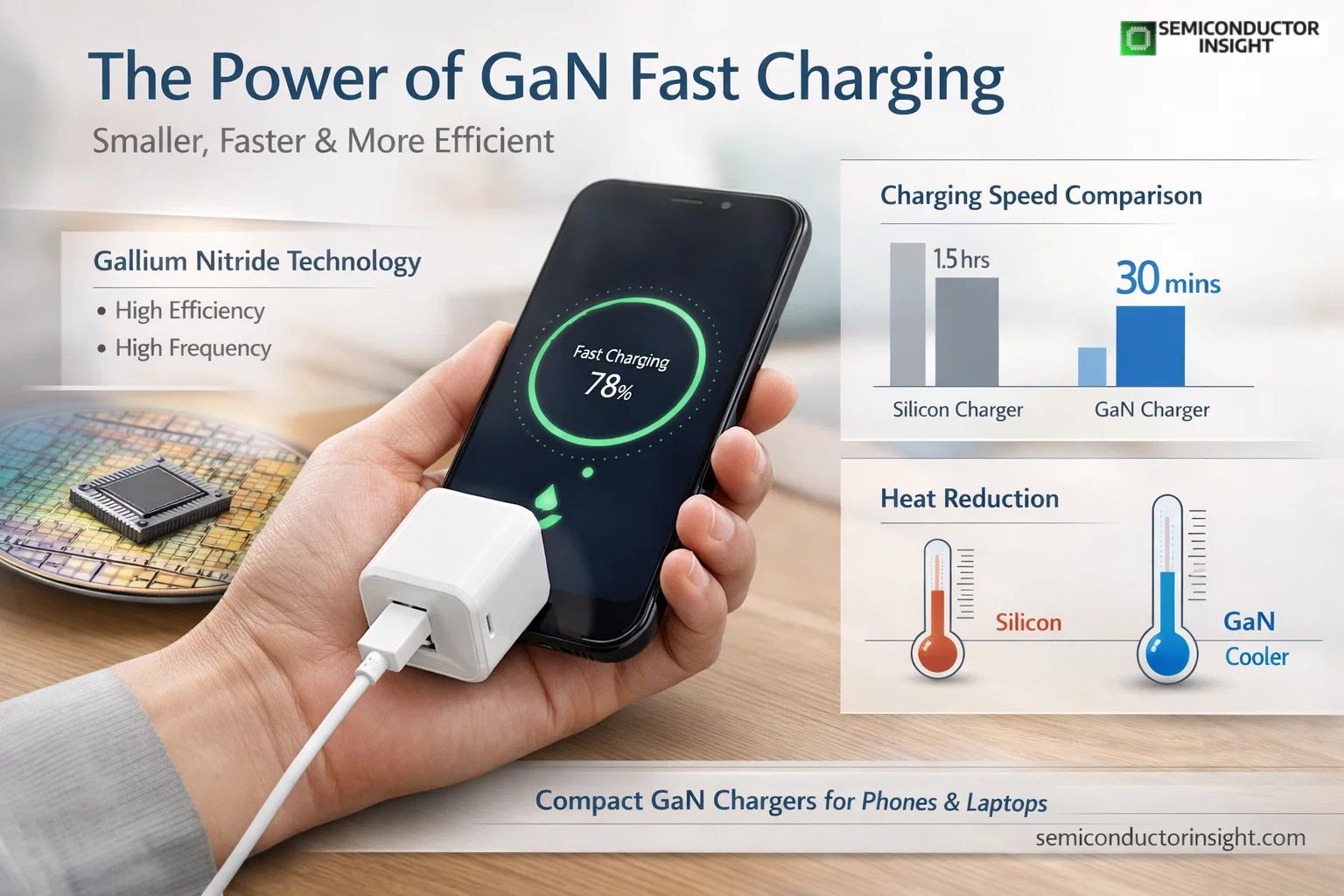
Heat has always been the enemy of fast charging. Silicon chargers waste a good chunk of energy as warmth, forcing bigger heat sinks and bulkier casings. GaN chips flip that equation with efficiencies that routinely top 95%, meaning most of the power goes straight to your battery instead of warming up the charger. Anker’s own engineering notes highlight how GaN handles higher voltages and conducts electricity more efficiently, wasting less energy as heat even at 65 watts or 100 watts output.
A typical 65 watt GaN charger can bring many smartphones to 50% in around 30 minutes and fully charge laptops in well under two hours, all while staying noticeably cooler to the touch. That lower thermal load also improves long term reliability, with some GaN based designs reporting failure in time rates as low as 0.54 FIT and mean time to failure stretching beyond 233 years in real world charger applications.
Bringing It Home GaN in the Chargers You Use Every Day
- Walk into any electronics store and you will spot the difference immediately. Brands like Anker, Belkin, Xiaomi, Samsung, Lenovo, and OPPO have rolled out GaN powered chargers that feel almost weightless compared to their older silicon cousins.
- A 30 watt GaN USB PD wall charger is dramatically smaller than a comparable silicon model, yet it supports the full range of Power Delivery and Quick Charge protocols that modern phones and tablets demand.
- EPC, another leader in GaN technology, points out that these devices offer higher breakdown strength, faster switching, and lower on resistance, which translates directly into compact multi-port chargers that can simultaneously top up a laptop, phone, and earbuds without breaking a sweat.
- Travelers love them because the same power output now fits in a pocket, and home users appreciate the clean desk space and reduced cable clutter.
Pushing Boundaries Semiconductor Innovations Fueling GaN Fast Charging
Engineers keep refining GaN power ICs with features like integrated sensing and autonomous protection that react in nanoseconds to over current or over temperature conditions. These advances make the chips not just faster but genuinely smarter, protecting both the charger and the connected device without relying on extra external circuitry. The semiconductor industry has also optimized GaN on silicon manufacturing processes, keeping costs competitive while delivering performance that was once reserved for exotic materials.
The fast charging GaN chips market keeps evolving because every new generation squeezes more power density into smaller packages, opening doors for everything from ultra portable laptop adapters to high wattage multi device hubs that feel like they belong in a sci fi movie. Next time you plug in and watch the battery%age climb at lightning speed, remember it is the tiny GaN chip inside doing the heavy lifting with elegance and precision that older silicon technology could never match.
Comments (0)