
Precision Spectroscopy and Attenuated Total Reflection Probes Market in Semiconductors
Attenuated total reflection probes have quietly become essential allies in the fast-paced world of semiconductor fabrication, where every angstrom counts toward higher yields and smaller nodes. Without requiring complicated sample preparation, these fiber-optic or crystal-based sensors use the evanescent wave produced during total internal reflection to yield molecular fingerprints straight from liquids, slurries, or thin films.
For fab teams pushing 3nm and below processes, this means instant feedback on chemical composition right at the point of use whether monitoring etch baths, CMP slurries, or post-clean residues on wafers. The technique’s surface sensitivity, typically penetrating just 0.5 to 5 micrometres depending on wavelength and incidence angle, aligns perfectly with the ultra-thin layers and interfaces that define today’s devices.
Evanescent Waves at Work: Surface Sensitivity Tailored for Semiconductor Metrology
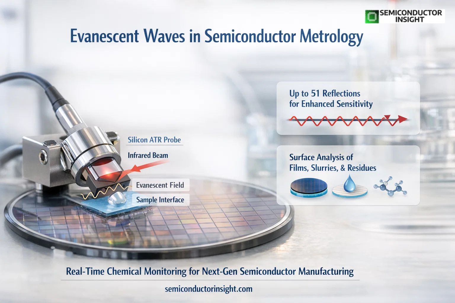
- Consider an infrared beam moving through a crystal with a high refractive index or a doped silicon wafer.
- At the interface with your process fluid or coated surface, part of the energy extends as an evanescent field that interacts only with the immediate contact layer. This creates sharp absorption peaks for functional groups in photoresists, cleaning agents, or contaminants without the beam passing through the entire bulk sample.
- In semiconductor labs and production floors, multiple-reflection setups take this further.
- A 0.77 mm-thick silicon wafer as the internal reflection element can produce up to 33 bounces, while a 0.50 mm version delivers 51, dramatically boosting signal strength for trace detection.
- Researchers at academic and national labs have documented how this setup identifies organic residues at levels critical for gate oxide integrity, often below 5.3 × 10^13 carbon atoms per square centimetre as referenced in industry roadmaps.
- The result is cleaner data on surface chemistry that directly correlates to device performance, helping engineers tweak processes before defects cascade downstream.
Smart Optical Measurement Using Chip-Grade Materials for Scalable Production Environments
One of the smartest evolutions in this space comes from treating standard silicon wafers themselves as the ATR crystal. A previous study published in Analytical Chemistry demonstrated that a simple diced or cleaved Silicon wafer piece serves as a disposable internal reflection element no polishing, no expensive diamond or germanium crystals needed. This approach cuts costs while maintaining compatibility with the very substrates running through your fabs.
More recent work in 2023 from the Journal of Sensors and Sensor Systems introduced compact silicon-based ATR sensor modules designed for continuous industrial operation. These rugged units handle aggressive cleaning-in-place chemicals, abrasive slurries, and temperature swings up to 280°C, conditions that mirror the wet benches and CMP tools in semiconductor lines. For process engineers, the payoff is immediate: real-time concentration tracking of isocyanates or other reactive species in liquid mixtures, with measurements stable enough for closed-loop control.
Diamond-Coated Silicon ATR Probes: Durability Engineered for Aggressive Semiconductor Chemistries
When standard silicon needs extra toughness, diamond coatings step in. A 2021 investigation in Sensors detailed nanocrystalline diamond layers applied to silicon ATR elements, extending sensor lifetime in corrosive etch and clean environments while preserving infrared transparency.
The coating thickness and incidence angle can be tuned so absorbance scales predictably, giving reliable quantitative data even after repeated exposure to hydrofluoric acid mixtures or alkaline developers. In practical terms, fabs gain probes that survive hundreds of process cycles without drift, reducing downtime and calibration overhead. This durability directly supports the move toward longer runs between maintenance in 300 mm and emerging 450 mm wafer lines.
Before Proceeding, Feel Free to Overlook Our Updated Report: https://semiconductorinsight.com/report/attenuated-total-reflection-probes-market/
Transforming Silicon-Based Infrared Analysis for Next-Gen Manufacturing Environments
- A standout 2023 advance from the Journal of Physical Chemistry C showed how surface-proximal doping of silicon ATR crystals n-type or p-type in the top 100-200 nm turns the crystal into both optical element and working electrode.
- This enables operando monitoring of molecular redox processes right on the semiconductor surface under applied potential.
- For semiconductor teams exploring new gate stacks or catalytic surface treatments, the technique captures vibrational changes in monolayers without air exposure or separate electrodes.
- Early adopters report clearer insights into interface chemistry during plasma or wet processing, data that feeds directly into process optimization models. Combined with fiber-optic delivery, these probes now extend from benchtop validation to pilot-line integration.
Linking ATR Advances to High-Volume Manufacturing Wins
Semiconductor professionals using these probes consistently report tighter process windows and fewer yield excursions. Whether you operate a logic fab chasing 2nm targets or a memory facility scaling 3D stacks, attenuated total reflection probes translate raw spectral data into actionable control parameters.
The technology’s non-destructive nature and minimal footprint make it ideal for integration with existing toolsets, supporting the industry’s push for smarter, greener production. As nodes shrink and materials diversify, the attenuated total reflection probes market continues to deliver the molecular-level visibility that keeps yields climbing and costs under control.

Comments (0)