
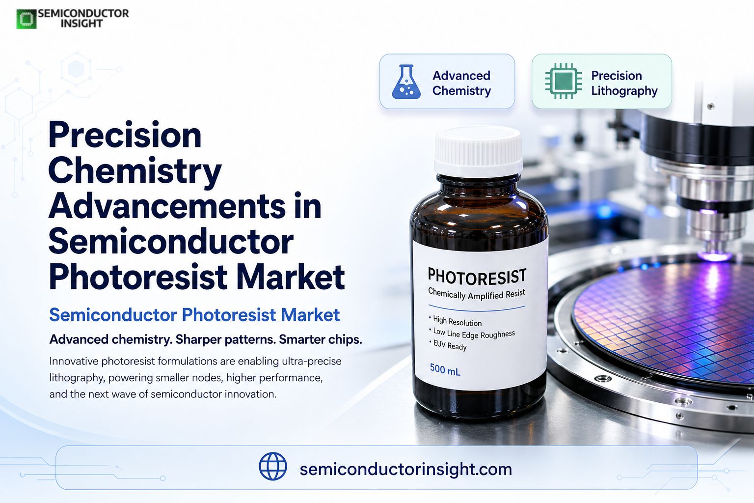
Precision Chemistry Advancements in Semiconductor Photoresist Market
Semiconductor photoresists serve as the light-sensitive gatekeepers in the intricate dance of photolithography, the process that literally writes the billions of transistors onto silicon wafers. These specialized polymer formulations undergo precise chemical transformations when exposed to specific wavelengths of light, allowing manufacturers to transfer complex circuit patterns from photomasks onto the wafer surface with extraordinary accuracy.
In fabs around the world, technicians apply a thin layer of this material via spin coating, typically dispensing between 1.5 and 5 millilitres per 300mm wafer, before soft-baking, exposing, developing, and etching. Only a small fraction often around 6-7% remains on the wafer after processing, with the rest spun off and handled as waste.
The chemistry behind these materials is sophisticated. Traditional positive photoresists, based on novolac resins and diazonaphthoquinone (DNQ) sensitizers, become more soluble upon exposure. Negative resists crosslink and harden in exposed areas. For advanced nodes, chemically amplified resists (CARs) dominate, using photoacid generators (PAGs) that trigger catalytic reactions, amplifying the effect of each photon and enabling the extreme sensitivity required for deep ultraviolet (DUV) and extreme ultraviolet (EUV) lithography.
Core Composition and Polymer Backbone
- At the molecular level, photoresists blend a base resin (providing film-forming and etch-resistance properties), a photoactive compound or PAG, and solvents that control viscosity for uniform coating.
- Common solvents include propylene glycol monomethyl ether acetate (PGMEA).
- For DUV applications, polymers like polyhydroxystyrene (PHS) for KrF (248 nm) or acrylic-based systems for ArF (193 nm) deliver the necessary transparency and performance.
- EUV resists at 13.5 nm often incorporate metal-organic frameworks or high-absorbance elements to better capture the low-photon-count exposure.
- These formulations must balance sensitivity, resolution, line-edge roughness, and etch selectivity while maintaining purity levels measured in parts per billion.
The Lithography Process Integration
In a typical high-volume fab, a single wafer can undergo 50 or more lithography steps as layers stack to create transistors, interconnects, and vias. Global semiconductor capacity has surpassed 30 million 300mm equivalent wafers per month, translating into enormous cumulative demand for photoresist materials across thousands of process layers.
Each step involves precise control of film thickness often 50 to 200 nanometers spin speed, bake temperatures, and exposure doses measured in millijoules per square centimeter. Immersion lithography with water between the lens and wafer boosts resolution for ArF systems, while EUV tools operate in vacuum with reflective multilayer mirrors.
To Stay Tuned with More meaningful and In-Depth Insights, Do Visit here: https://semiconductorinsight.com/report/nand-flash-memory-and-dram-market/
Wavelength-Specific Material Innovations
Different wavelengths demand tailored chemistries. G-line and I-line resists handled earlier micron-scale features, but today KrF and ArF systems pattern features well below 100 nm, often with multiple patterning techniques. EUV lithography pushes boundaries further, enabling single-exposure patterning at sub-10 nm nodes.
Recent developments include non-fluorinated platforms for sustainability and metal-oxide resists that offer higher etch resistance and lower line-edge roughness for the most demanding applications. These innovations address stochastic noise and photon shot noise inherent at EUV wavelengths.
Current Industry Realities and Technical Demands
- Modern fabs operate around the clock with stringent cleanroom controls to prevent a single particle from ruining patterns.
- Photoresist purity, batch-to-batch consistency, and compatibility with new hardware are non-negotiable. Suppliers work closely with foundries like TSMC, Samsung, and Intel to qualify materials for each technology node.
- Challenges around stochastic effects in EUV, reducing defects, and improving process windows drive ongoing R&D into novel polymer architectures and hybrid materials.
- Sustainability efforts focus on lowering solvent use and developing greener formulations without compromising performance.
Semiconductor Photoresist Market sits at the intersection of organic chemistry, materials science, and Nano scale engineering. These specialized formulations continue to evolve, quietly enabling the exponential increases in computing power that define our digital age. As chipmakers pursue ever-smaller features and more complex 3D architectures, the precision chemistry of photoresists remains indispensable to turning silicon wafers into the powerful processors shaping tomorrow’s technology.

Comments (0)