
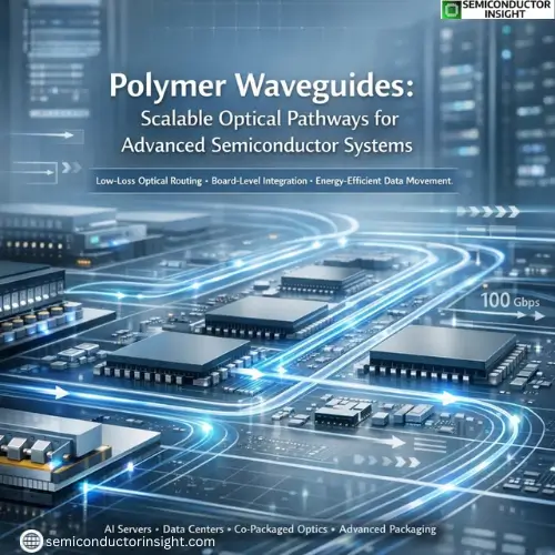
Polymer Waveguide Market Analysis: Optical Performance Meets Manufacturing Flexibility
As semiconductor systems confront physical limits of copper interconnects, the industry is accelerating toward optical signal pathways that can sustain speed, bandwidth, and energy efficiency. Polymer waveguides have emerged as a practical solution, delivering optical performance without the cost and rigidity associated with traditional glass-based photonics.
Rather than competing with silicon photonics, polymer waveguides complement it serving as short-range, board-level, and chip-to-module optical highways that support modern data movement.
What Defines a Polymer Waveguide System?
Polymer waveguides are optical transmission paths fabricated from engineered polymer materials that guide light with minimal loss over short to medium distances. Their ability to be patterned directly onto substrates, combined with flexible processing methods, makes them especially attractive for high-density semiconductor packaging.
Core attributes shaping adoption include:
- Low optical attenuation at short distances
- Compatibility with PCB and substrate manufacturing
- Reduced alignment sensitivity compared to glass fibres
- Mechanical flexibility supporting compact system layouts
These advantages align well with the evolving needs of data centres, high-performance computing, automotive electronics, and telecom infrastructure.
Technology Momentum: Why Polymers Are Gaining Preference
The growing complexity of semiconductor systems has intensified the demand for energy-efficient interconnects. Polymer waveguides help reduce electrical-to-optical conversion losses while enabling parallel optical channels within confined spaces.
Key technical drivers accelerating uptake:
- Rising data rates beyond copper interconnect limits
- Increased thermal density in advanced semiconductor nodes
- Need for cost-effective optical routing inside electronic assemblies
As packaging architectures evolve, polymer waveguides are becoming an integral component rather than an experimental add-on.
Application Expansion across Semiconductor Ecosystems
Demand is being shaped by use cases where optical efficiency directly influences system performance:
- Data centres & AI servers, where polymer waveguides support board-level optical links
- Telecom switching equipment, enabling compact and scalable signal routing
- Automotive electronics, particularly ADAS and sensor fusion systems
- Advanced packaging platforms, including co-packaged optics
These applications value manufacturing scalability and integration ease, areas where polymer waveguides outperform rigid alternatives.
Competitive Landscape: Key Players and Strategic Positioning
The polymer waveguide market is characterized by material innovators, photonics specialists, and semiconductor packaging partners.
Notable players active in this space include:
- Dow (polymer materials development)
- Shin-Etsu Chemical
- Corning (hybrid optical material strategies)
- AGC Inc.
- Sumitomo Bakelite
- Broadcom (system-level optical integration)
- Hamamatsu Photonics
Strategic focus areas observed among leading companies:
- Development of low-loss polymer formulations
- Partnerships with semiconductor packaging houses
- Integration with silicon photonics platforms
- Custom waveguide solutions for hyper scale customers
Rather than competing on price alone, companies are emphasizing optical performance, process compatibility, and long-term reliability.
For a more thorough report, please contact us using our most recent report:
https://semiconductorinsight.com/report/polymer-waveguide-market/
Current Industry Circumstances Affecting Market Direction
Recent developments indicate a clear shift toward co-packaged optics and optical I/O architectures, where polymer waveguides act as a bridge between chips and external fibre links. Several semiconductor manufacturers are piloting polymer-based optical routing in next-generation compute platforms, signalling growing commercial confidence.
At the same time, supply chain resilience has become a priority, encouraging regional material sourcing and localized production capabilities.
Manufacturing Economics and Scalability
One of the strongest arguments for polymer waveguides lies in their manufacturing economics. Unlike glass-based systems requiring precision assembly, polymer waveguides can be fabricated using scalable processes such as photolithography, embossing, and printing.
This supports:
- Higher production yields
- Lower assembly costs
- Faster design iteration cycles
For system integrators, these factors translate into shorter time-to-market and improved design flexibility.
Upcoming Scope for Competitors and New Entrants
The next growth phase of the polymer waveguide market will be shaped by:
- Expansion into AI accelerator platforms
- Integration with advanced substrates and interposers
- Development of high-temperature and low-loss polymer variants
- Increased adoption in automotive and industrial electronics
New entrants with strengths in materials science, photonics design, or semiconductor packaging services can carve out niche positions by addressing application-specific optical challenges.
Investor Focused Market Summary
Polymer waveguide market represents a structural shift in how data moves within semiconductor systems. Its value lies not in replacing existing optical technologies, but in enabling scalable, cost-efficient optical integration at the board and package level.
For investors, the market offers:
- Exposure to long-term growth in optical interconnects
- Alignment with AI, data centre, and advanced packaging trends
- Opportunities driven by materials innovation and system-level adoption
As semiconductor architectures evolve toward optical-first designs, polymer waveguides are positioned as a foundational technology rather than a peripheral component.

Comments (0)