
Polar Orbit Deployments Validating Durability for MEMS Thermopile Temperature Sensor Market Deployments
Engineers working at the intersection of semiconductors and thermal sensing have turned to MEMS thermopile technology to capture temperature differences without ever touching the surface. These tiny devices rely on the Seebeck effect, where a chain of thermocouples connected in series generates a measurable voltage whenever infrared radiation heats one set of junctions while the other stays cooler.
Fabricated directly on silicon wafers using standard semiconductor processes, they shrink what used to require bulky optics into microscopic packages that fit inside smartphones, industrial tools, and even shoebox sized satellites.
The Semiconductor Heart of Thermopile Temperature Sensing
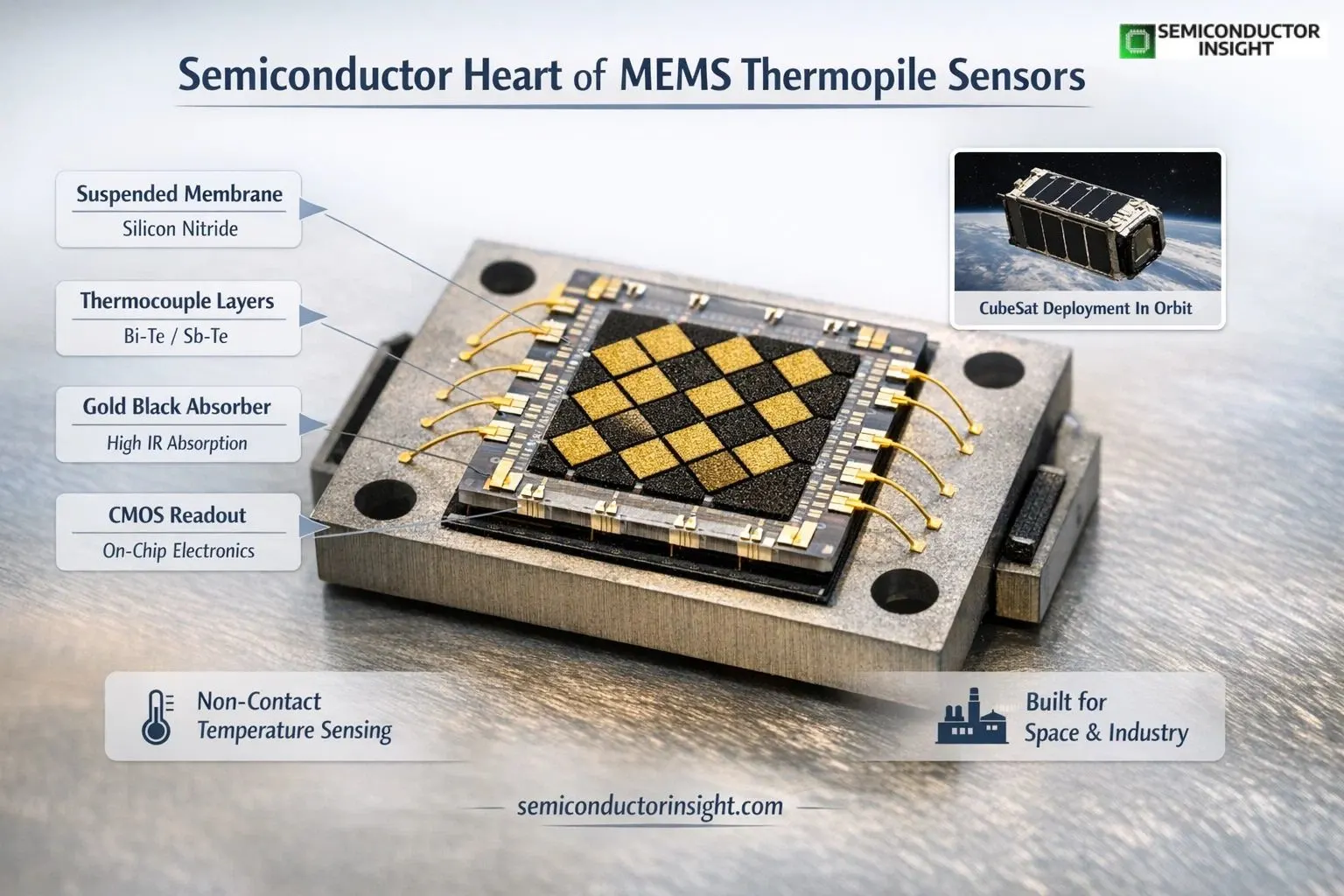
At the core sits a micromachined silicon structure that isolates heat flow with remarkable precision. Thin films of carefully chosen thermoelectric materials form the thermocouples, while suspended absorbers capture incoming infrared energy and convert it into a tiny temperature gradient.
Because the entire sensor is built in a cleanroom environment alongside conventional CMOS circuitry, designers can embed signal conditioning right on the same chip, reducing noise and simplifying system integration for everything from handheld thermometers to automated manufacturing lines.
Explore the complete report here for deeper insights: https://semiconductorinsight.com/report/mems-thermopile-temperature-sensor-market/
Micromachining Techniques That Create Suspended Thermal Structures
The magic happens through deep reactive ion etching and surface micromachining that release delicate membranes and beams only a few micrometers thick. These freestanding elements minimize heat loss to the substrate, allowing the sensor to respond quickly to subtle temperature shifts.
Gold black coatings applied to the absorber surface ensure nearly complete absorption across a wide infrared band, turning each pixel into an efficient radiation trap without the need for external lenses in many designs.
NASA CubeSat Deployments Showcasing Sensor Reliability in Orbit
- In 2024 two PREFIRE CubeSats lifted off on Rocket Lab Electron rockets in May and June, each carrying a custom thermopile detector array built from bare silicon at NASA’s Jet Propulsion Laboratory Microdevices Laboratory.
- The 64 by 8 pixel array, the highest density of its kind produced there so far, features a diamond pattern micromachined layout that cuts noise by 30 to 50% through reduced capacitance.
- Suspended silicon nitride absorbers sit on four support beams, each wired with n type bismuth telluride and p type antimony telluride layers, while a central gold black coating delivers near perfect optical efficiency from 5 to 45 micrometers.
- These sensors now orbit Earth’s poles, feeding back far infrared data that helps climate scientists understand how clouds and water vapor influence heat loss in Polar Regions.
Material Choices Optimizing Seebeck Effect in Miniature Devices Bismuth antimony telluride pairs stand out because their high Seebeck coefficients deliver strong voltage signals even from modest temperature differences. Single crystal silicon alternatives or polysilicon aluminum stacks offer CMOS compatibility for lower cost runs, while the choice of support materials like silicon nitride keeps thermal conductance low. Each combination is tuned so the sensor maintains stability across the temperature swings encountered in space or factory floors.
Step by Step Fabrication Journey from Bare Silicon to Integrated Sensor
Fabrication begins with a standard silicon wafer.
↓
Deep reactive ion etching releases the suspended membranes and support beams.
↓
Thermoelectric layers are deposited and patterned to form the thermocouple chains.
↓
Gold black absorber coating is applied selectively to the hot junctions.
↓
Readout integrated circuits are bonded or monolithically integrated.
↓
Final packaging seals the focal plane module for flight or industrial use.
This sequence keeps costs down and yields high because it leverages the same tools already running 24 hours a day in semiconductor foundries worldwide.
Design Features That Minimize Noise and Maximize Optical Efficiency
MEMS thermopile sensors are built with carefully selected components that work together to reduce noise and improve optical efficiency. The absorber membrane is typically made of silicon nitride for low thermal mass and fast response, while thermocouple wires use Bi-Sb-Te to deliver a high Seebeck coefficient. A gold black coating helps achieve near 100% IR absorption, and micromachined silicon support beams provide strong thermal isolation with minimal noise. The readout circuitry is CMOS integrated, allowing on-chip amplification and filtering for more stable performance.
Together, these elements enable the sensor to detect temperature changes in real time while withstanding launch vibrations, radiation exposure, and years of continuous operation. This makes the technology highly reliable for non-contact measurements in environments where traditional probes are not practical. From monitoring wafer temperatures during semiconductor processing to tracking planetary heat balance from orbit, MEMS thermopile sensors continue to show how small devices can deliver powerful insights.

Comments (0)