
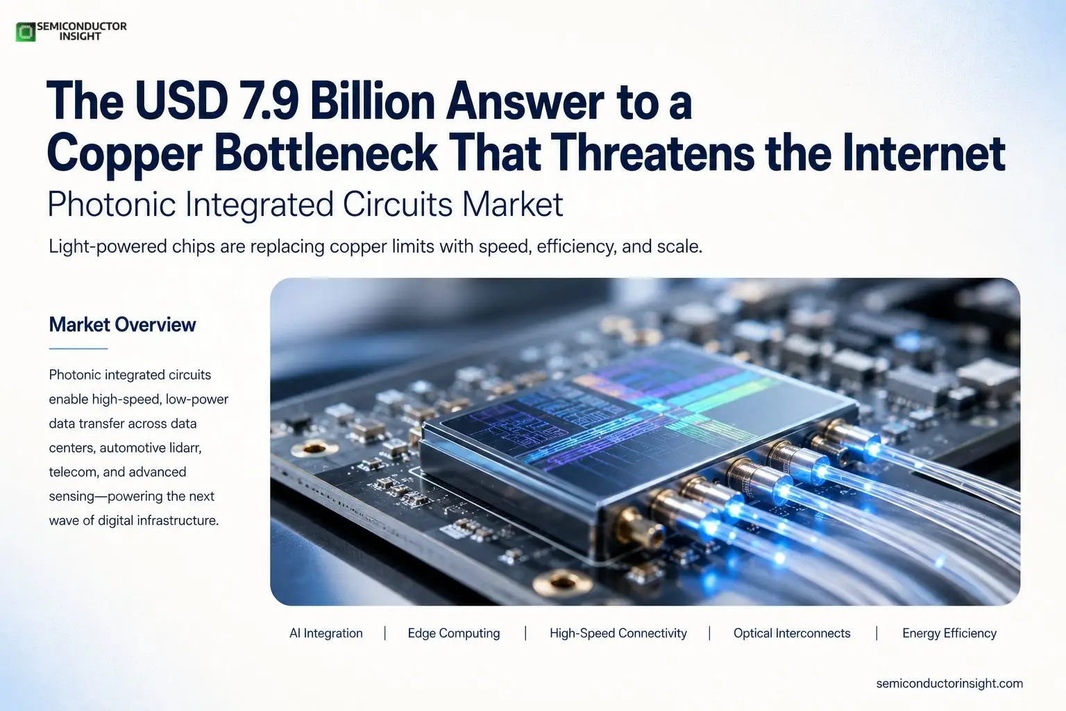
Photonic Integrated Circuits Market 2026: The USD 7.9 Billion Answer to a Copper Bottleneck That Threatens the Internet
In a data centre somewhere in northern Virginia, a rack of servers is humming through the evening. The processors inside are unthinkably fast, capable of crunching billions of operations per second. But the real bottleneck is not the chips themselves; it is the wires that connect them. Copper traces, however finely engineered, are reaching their physical limits. They get hot, they sap power, and they struggle to push data fast enough to keep modern workloads – large language models, real‑time video analytics, genomic simulations – from stalling. In 2026, the escape route from this bottleneck looks increasingly like a beam of light.
Photonic integrated circuits, or PICs, use photons instead of electrons to move information. They are fabricated on silicon, indium phosphide, or other semiconductor substrates, and they integrate lasers, modulators, waveguides, and detectors onto a single chip, much the way an electronic IC crams billions of transistors onto a sliver of silicon. The difference is that light can carry vastly more data, over longer distances, with a fraction of the heat. The market for these devices, valued at roughly USD 7.9 billion in 2025, is now on a trajectory that analysts expect will take it to USD 24.8 billion by 2034. That implies a compound annual growth rate of around 13.5 percent, a pace that belongs to a technology in the process of being pulled from niche applications into the infrastructure backbone of the digital economy.
The data centre wakes up to its power problem
The single biggest force behind that growth is the hyperscale data centre. Global data-centre traffic is expected to surpass 120 exabytes per year by 2028, according to industry forecasts that now look conservative. Every exabyte is a billion gigabytes, and every gigabyte shuttled across a copper interconnect inside a server farm consumes a measurable amount of electricity and generates a measurable amount of heat. When a campus contains hundreds of thousands of servers, the interconnect power alone can rival the consumption of a small city.
Photonic chips change the arithmetic. In the kinds of high‑speed, short‑reach links that connect switches, routers, and compute blades, silicon photonics can cut power consumption by as much as 70 percent compared with equivalent copper solutions. That number is not a laboratory claim; it has been validated in field deployments and is now appearing in the procurement criteria of the world’s largest cloud operators. A 70 percent reduction in interconnect power, multiplied across a million links, shifts the economics of data-centre design. It frees up electrical capacity for more compute, reduces cooling requirements, and helps operators stay within the emission envelopes that regulators and shareholders are beginning to enforce.
In March 2026, a major hyperscaler – one of the handful that collectively drive the bulk of global server demand – quietly disclosed in a technical blog that its newest data centre campus in Oregon was running photonic interconnects across its entire high‑bandwidth fabric. The company claimed a 65 percent reduction in interconnect energy per bit compared with its previous copper‑based design, and it suggested that the technology would be standard in all future greenfield builds. The announcement, covered by several networking trade publications, sent a clear signal through the supply chain: photonic integration had moved from an interesting option to a default specification for the largest buyers of interconnect technology.
What a photonic integrated circuit actually does
To understand why this matters, it helps to picture what a PIC replaces. In a traditional optical transceiver, the kind that plugs into a switch port, the laser, modulator, and photodetector are discrete components assembled on a circuit board. This works, but it is bulky, power‑hungry, and expensive to manufacture at scale. A photonic integrated circuit takes all those functions and etches them onto a single chip using wafer‑scale processes that borrow heavily from the semiconductor industry’s playbook. The result is a device that can be stamped out by the thousands on a silicon wafer, tested at the wafer level, and packaged into a module the size of a fingernail.
Silicon photonics, in particular, has benefited from the fact that it can be manufactured in existing CMOS fabs with relatively modest modifications. That compatibility with the semiconductor supply chain is what allows companies to talk seriously about producing millions of PICs per year. It is also what makes the 24.8 billion‑dollar projection plausible rather than aspirational.
Beyond the data centre: lidar, sensing, and the next frontiers
While data‑centre interconnects are the largest near‑term driver, they are not the only one. Photonic integrated circuits are also becoming central to lidar systems for autonomous vehicles and industrial robotics. A photonic chip can steer a laser beam without moving parts, scanning the environment at speeds and resolutions that mechanical lidar cannot match. Several automotive‑grade lidar suppliers now use PICs as the optical engine in their sensors, and as vehicle autonomy programmes advance – albeit more slowly than the hype once predicted – the demand for these chips is growing steadily.
In biosensing and medical diagnostics, PICs enable compact, label‑free detection of proteins, pathogens, and chemical markers by measuring minute changes in the refractive index on a chip surface. The COVID‑19 pandemic spurred investment in photonic biosensors, and in 2026, point‑of‑care diagnostic platforms using silicon nitride waveguide chips are being trialled in hospitals in the Netherlands and Singapore. The volumes here are modest compared with data‑centre transceivers, but the value per chip is high, and the societal need is clear.
Then there are the emerging applications that are still in the research phase but carry the potential to reshape the market in the second half of the forecast period. Optical computing, where photonic chips perform matrix multiplications for AI inference at speeds and energy efficiencies that electronic processors cannot approach, is attracting serious venture funding. Several startups have demonstrated photonic tensor cores in the lab, and while a general‑purpose optical computer remains a distant goal, the integration of photonic co‑processors into specific AI acceleration tasks is starting to look less like science fiction and more like a near‑term engineering challenge.
The manufacturing challenge that keeps everyone honest
For all the promise, photonic integrated circuits are not trivial to build. The waveguides must be etched with nanometre precision, the coupling between laser sources and silicon chips must be nearly lossless, and the packaging – the step where a photonic chip is connected to optical fibres and electrical drivers – remains a significant cost driver. Unlike electronic chips, which can tolerate a certain amount of heat and variability, photonic circuits are exquisitely sensitive to temperature fluctuations and fabrication tolerances. The industry has made enormous progress in wafer‑scale testing and automated alignment, but the yield and packaging hurdles are the main reason the market is still measured in billions rather than tens of billions.
The supply chain is also concentrated. A relatively small number of foundries, mostly in the United States and Europe, offer true silicon photonics processes. The reliance on advanced CMOS nodes for the electronic control circuitry that accompanies a photonic chip means that the same geopolitical tensions affecting the broader semiconductor industry also cast a shadow here. Governments are beginning to notice. The U.S. CHIPS Act and the European Chips Act both include funding streams for photonics research and manufacturing, reflecting a growing recognition that the ability to produce photonic chips domestically is as strategically important as the ability to produce advanced processors.
Where the market is heading
The path from 7.9 billion dollars in 2025 to 24.8 billion in 2034 will not be a straight line. It will be shaped by the investment cycles of cloud providers, the adoption tempo of lidar in vehicles, and the unpredictable pace at which optical computing matures. But the fundamental reason to be optimistic about the market is that copper is running out of headroom. The bandwidth demands of AI, streaming, and cloud computing are doubling every two to three years, and copper cannot keep up without consuming an unacceptably large share of the energy budget. Photons, once confined to long‑haul telecom fibres, are moving inside the server rack, onto the board, and eventually onto the chip package itself. Each step inward opens a new market.
In 2026, the photonic integrated circuits market is where the solid‑state drive market was in the late 2000s – no longer a niche, not yet universal, but clearly on the right side of history. The companies that master the manufacturing and packaging challenges will find themselves supplying the nervous system of the digital world, one that runs on light instead of electrons. The 24.8-billion-dollar number is a forecast, but the direction of travel is, quite literally, at the speed of light.
Read the Full Report for Key Data: https://semiconductorinsight.com/report/photonic-integrated-circuits-market/

Comments (0)