
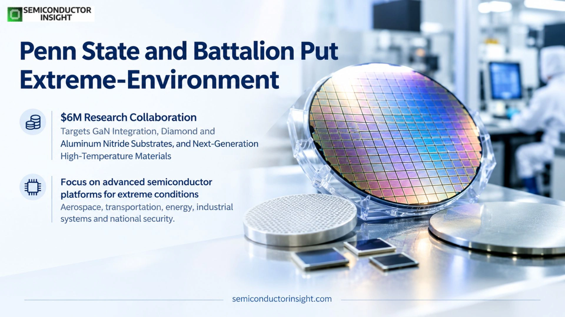
Penn State and Battalion Put Extreme-Environment Semiconductor Technology on the National Security Agenda
$6M Research Collaboration Targets GaN Integration, Diamond and Aluminum Nitride Substrates, and Next-Generation High-Temperature Materials
The semiconductor industry’s next performance gains may depend not only on smaller devices, but on how effectively advanced chips can survive, operate and dissipate heat under extreme conditions.
A new research collaboration between Penn State University and UK-based Battalion Advanced Technology Ltd. is targeting exactly that challenge. The two organizations have entered into research agreements worth up to $6 million to advance semiconductor platforms and high-temperature materials designed for demanding applications spanning aerospace, transportation, energy, industrial systems and national security.
The Semiconductor Challenge Is Moving Beyond Device Performance
As power electronics, aerospace systems and defense platforms demand higher power density and faster operation, conventional semiconductor architectures face a fundamental obstacle: heat and material compatibility.
Penn State researchers are therefore investigating ways to combine gallium nitride (GaN) and related wide-bandgap and ultrawide-bandgap semiconductors with substrates capable of providing substantially stronger thermal and electrical performance.
The research is being led by Joan Redwing, distinguished professor of materials science and engineering and electrical engineering at Penn State.
The objective is ambitious develop a pathway for integrating advanced semiconductor layers with materials such as diamond and aluminum nitride, both attractive for their thermal-management capabilities but challenging to integrate directly with semiconductor materials.
Why Diamond and Aluminum Nitride Matter?
For high-power semiconductor systems, getting heat away from the active device is becoming just as important as improving the device itself.
Diamond is particularly attractive because of its exceptional thermal conductivity, while aluminum nitride offers a combination of thermal performance and electrical insulation that can benefit advanced power and RF applications.
However, integrating dissimilar crystalline materials can introduce:
- Lattice and thermal-expansion mismatches
- Interfacial defects
- Mechanical stress
- High thermal resistance at material boundaries
- Difficulties in achieving high-quality crystalline growth
The Penn State-Battalion program is exploring whether atomically thin two-dimensional materials can act as engineered interlayers between these materials.
Two-Dimensional Materials Enter the Semiconductor Integration Picture
Rather than relying exclusively on conventional direct-growth techniques, researchers will examine whether ultra-thin interlayers can create a more favorable interface between GaN and high-thermal-conductivity substrates.
The approach could potentially reduce crystalline defects and interfacial thermal resistance, while helping enable semiconductor growth on substrates that have historically been difficult to combine directly.
This is significant because the value of a high-performance semiconductor can be limited if the surrounding material architecture cannot effectively manage the heat generated during operation.
The research will combine materials synthesis, advanced characterization, computational analysis and semiconductor engineering, drawing on Penn State’s Materials Research Institute and its wider interdisciplinary research infrastructure.
From Laboratory Materials to Strategic Hardware
- The collaboration has a broader dimension beyond semiconductor fabrication.
- The research is being positioned around technologies that need to function under extreme temperature, power and environmental conditions.
- Such requirements are particularly important in aerospace and defense systems, where reliability can be as critical as speed or efficiency.
- Penn State’s Materials Research Institute director Joshua A. Robinson emphasized that combining semiconductor science, computation, and manufacturing and characterization capabilities creates an interdisciplinary platform for addressing materials challenges tied to technological leadership and national security.
- The collaboration therefore sits at the intersection of advanced semiconductor materials and dual-use technology development.
The $6M Program Has a Second Materials Front;
While the semiconductor research is focused on GaN integration and thermal-performance challenges, the broader collaboration also addresses another extreme-environment problem: high-temperature materials for applications including hypersonic flight.
Researchers will investigate durable, oxidation-resistant alloys capable of maintaining performance under extreme temperatures.
Together, the two projects address complementary requirements for future strategic technologies:
- Advanced semiconductor platforms → higher electrical and thermal performance
- Extreme-temperature alloys → greater durability in severe operating environments
Why This Matters to the Global Semiconductor Industry?
The collaboration arrives as semiconductor development increasingly expands beyond traditional metrics such as transistor density and process-node scaling.
For high-power electronics, RF systems, electric transportation, aerospace platforms and defense applications, the competitive advantage increasingly depends on materials engineering, thermal management and heterogeneous integration.
GaN and other wide-bandgap technologies are already attracting attention because of their potential for high-frequency and high-power operation. Pairing them with advanced thermal substrates could open another avenue for improving system-level performance.
If successful, Penn State and Battalion’s research could help address one of the semiconductor industry’s persistent bottlenecks: how to combine materials with very different properties without sacrificing reliability, heat transfer or crystal quality.
- The significance of the agreement extends beyond its $6 million headline value.
- It represents a broader shift toward materials-led semiconductor innovation, where breakthroughs in interfaces, substrates and thermal architecture can become as strategically important as advances in chip design.
- For the United States and its technology ecosystem, the research also reinforces the growing connection between semiconductor capability, advanced materials, aerospace and national security.
The next generation of high-performance chips may not be defined by the semiconductor alone but by the materials engineered around it.
A Brief Look at Our Detailed Analysis Related Report: https://semiconductorinsight.com/report/gallium-nitride-gan-wafer-foundry-market/

Comments (0)