NCSU Scientists Pioneer Laser Sintering Technique for Ultra-High-Temperature Ceramics
In the rapidly advancing world of industrial electronics and photonics, ceramic packaging has become a crucial enabler for high-performance applications. Ceramics offer unique advantages such as thermal stability, chemical resistance, and electrical insulation, making them indispensable in industries ranging from semiconductors to aerospace. With the integration of laser-based processing techniques, the industrial ceramic packaging sector is undergoing a wave of transformation, enabling more precise, energy-efficient, and versatile manufacturing capabilities.
The Industrial Laser Ceramic Package market, valued at USD 208 million in 2024, is projected to grow to USD 284 million by 2032, expanding at a CAGR of 4.5%. This steady growth is driven by technological breakthroughs in laser sintering, ultrafast welding, and ceramic additive manufacturing, alongside increasing adoption in sectors like defense, space exploration, electronics, and medical devices.
Access Your Free Sample Report- Industrial Laser Ceramic Package Market
Why Ceramic Packaging Matters
Before delving into the latest advancements, it’s important to understand why ceramic packaging holds such significance in industrial applications:
- Thermal Stability – Ceramics can withstand temperatures that would cause metals or polymers to degrade, making them essential for environments such as jet engines or hypersonic vehicles.
- Electrical Insulation – Unlike metals, ceramics are naturally insulating, making them ideal for use in high-power electronics.
- Corrosion Resistance – Ceramics do not oxidize or corrode easily, ensuring longevity in chemical processing and harsh environments.
- Mechanical Strength – Advanced ceramics like zirconia and alumina provide high fracture toughness, enabling durable packaging solutions.
- Miniaturization Potential – In consumer electronics and telecom, ceramic packages allow for high-density integration without thermal compromise.
Lasers complement these advantages by enabling precise machining, joining, and additive manufacturing without the need for mechanical tools or extreme furnace-based processes.
Market Snapshot: Growth Trajectory
- Market Size (2024): USD 208 million
- Projected Size (2032): USD 284 million
- CAGR (2024–2032):5%
Growth is supported by:
- Increasing demand for miniaturized and high-power electronic devices.
- Expanding aerospace and defense investments in hypersonics, where ultra-high-temperature ceramics are vital.
- Rising interest in laser-based manufacturing for ceramics, reducing costs and increasing scalability.
- Adoption in medical technology, particularly in implants and lab equipment packaging.
Recent Developments in Industrial Laser Ceramic Packaging
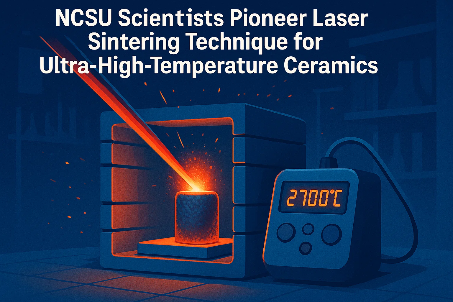
1. Laser Sintering of Ultra-High-Temperature Ceramics (NCSU Breakthrough)
Researchers at North Carolina State University (NCSU) have demonstrated a laser sintering process that creates hafnium carbide (HfC) ceramics from liquid polymer precursors. Traditionally, producing HfC required kilns operating above 2000°C, which limited scalability and material compatibility. By applying a 120-watt laser, NCSU scientists successfully transformed polymers into ceramics under localized conditions.
Why it’s a breakthrough:
- Energy Efficiency: Eliminates the need to heat an entire substrate in a furnace.
- Flexibility: Allows coatings on temperature-sensitive substrates, expanding application potential.
- Additive Manufacturing: Enables 3D printing of complex ceramic geometries.
- Industries Impacted: Aerospace (heat shields, hypersonic flight), nuclear energy (reactor liners), and electronics (high-temp packaging).
This approach marks a paradigm shift instead of bulk ceramic processing, manufacturers can now produce advanced ceramics in situ and on demand.
Download Sample Report PDF- Industrial Laser Ceramic Package Market
2. Laser Drilling Innovations by Laser Photonics (CMS Laser Expansion)
Laser Photonics Corporation (LPC), through its subsidiary CMS Laser, announced R&D expansion into laser drilling for ceramics. Traditional ceramic drilling involves mechanical methods prone to cracking and debris formation. The company’s new approach leverages high-precision, non-contact lasers to deliver clean, micro-scale holes with minimal damage.
Implications for the market:
- Semiconductors: Microvias in ceramic substrates for IC packaging.
- Medical Devices: Ceramic housings for sensors and implants.
- Automotive & Aerospace: Lightweight, durable parts requiring precise microholes.
By addressing one of ceramics’ long-standing challenges machinability LPC is positioning itself at the forefront of industrial laser processing.
3. Ultrafast Laser Welding for Ceramics (UC Riverside & UC San Diego)
Ceramic welding has historically been difficult due to brittleness and high melting points. In 2025, researchers at UC Riverside and UC San Diego pioneered ultrafast laser welding of ceramics. This method uses femtosecond laser pulses to induce nonlinear absorption, achieving localized melting and creating vacuum-tight joints.
Key outcomes:
- Strong, Reliable Joints: Suitable for high-pressure or vacuum environments.
- Miniaturization Potential: Applicable to microelectronics packaging.
- Cross-Industry Applications: Medical implants, microfluidics, optical devices, and defense systems.
This development is particularly relevant to industrial ceramic packaging, as it enables seamless integration of ceramic housings without adhesives or intermediary bonding layers.
4. Additive Manufacturing for Ceramic Packaging (Bosch & 3DCeram Webinar)
A March 2025 webinar hosted by Bosch Advanced Ceramics and 3DCeram showcased laser-based ceramic additive manufacturing for series production. The event emphasized the shift from prototyping to mass-scale deployment.
Highlights:
- 3D Printed Ceramic Components: From laboratory equipment to aerospace-grade insulators.
- Scalability: Advanced laser systems now allow batch manufacturing.
- Customization: Tailor-made packaging for electronics and industrial sensors.
This signals that ceramic additive manufacturing (AM), once a niche technology, is rapidly becoming a mainstream production method.
5. Kyocera’s Showcasing of Ceramic Solutions (Pittcon 2025)
At Pittcon 2025, Kyocera presented its innovations in ceramic manufacturing, focusing on multilayer direct bonding, additive manufacturing, and sapphire apertures. Kyocera’s role as a global leader in ceramic packaging makes its developments highly influential.
Notable advancements:
- Direct Bonded Ceramics: Offering superior electrical insulation for power modules.
- Sapphire-Based Components: High-transparency and durability for optical and laser applications.
- Additive Manufacturing Integration: Pushing ceramics into precision lab and industrial workflows.
Kyocera’s participation underscores the increasing visibility of ceramic packaging at international tech forums, affirming its relevance across industries.
Broader Industrial Implications
The convergence of lasers and ceramics is more than just a technological curiosity it has industrial-scale consequences:
- Aerospace & Defense
- Hypersonic vehicles and spacecraft require ultra-high-temperature ceramics (UHTCs).
- Laser sintering enables protective coatings on lightweight substrates.
- Electronics & Semiconductors
- Ceramic substrates for high-frequency chips benefit from laser drilling and welding.
- Miniaturization and reliability are enhanced through precision laser packaging.
- Medical Technology
- Ceramic housings for implants (pacemakers, biosensors) can now be laser-processed.
- Ultrafast welding enables hermetically sealed medical devices.
- Energy & Nuclear
- Reactor components made from UHTCs become easier to fabricate with laser sintering.
- High-strength ceramic joints enable safer, more durable energy systems.
- Industrial Equipment
- Laser additive manufacturing makes custom ceramic parts available on demand.
- Durable ceramic coatings improve wear resistance in heavy machinery.
Market Growth Drivers
- Miniaturization Trend: Increasing demand for compact, reliable packaging in electronics.
- Green Manufacturing: Laser processes consume less energy than traditional kilns.
- Defense Spending: Hypersonic and space projects fueling UHTC demand.
- Medical Applications: Rising adoption of biocompatible ceramic implants.
- Global Manufacturing Shift: Asia-Pacific leading ceramic production with Europe and the U.S. focusing on R&D.
Challenges Facing the Market
- High Initial Investment – Laser systems for ceramics require specialized infrastructure.
- Material Brittleness – Despite advances, ceramics remain difficult to handle.
- Standardization Gaps – Lack of universal standards for ceramic laser packaging slows adoption.
- Skilled Workforce – Specialized knowledge is required to operate laser-ceramic systems.
Click Here To Download Full Sample Report- Industrial Laser Ceramic Package Market
Future Outlook (2025–2032)
Looking ahead, the industrial laser ceramic package market will likely evolve in the following ways:
- Integration with AI & Automation: Laser systems enhanced with AI-driven monitoring for real-time defect detection.
- Hybrid Manufacturing: Combination of additive manufacturing and laser sintering for faster, scalable production.
- Sustainability Push: Reduced carbon footprint through energy-efficient laser processes.
- Defense & Space Expansion: Greater demand for UHTC coatings as hypersonic and space programs scale globally.
- Medical Revolution: Growth in laser-welded ceramic implants and microdevices.
The Industrial Laser Ceramic Package market stands at an exciting crossroads, merging the durability and versatility of ceramics with the precision and efficiency of lasers. From NCSU’s polymer-to-ceramic laser sintering breakthrough to Kyocera’s large-scale ceramic solutions, innovations are shaping the future of electronics, aerospace, defense, medical, and energy industries.
With the market projected to rise from USD 208 million in 2024 to USD 284 million by 2032 at a CAGR of 4.5%, the coming years will be defined by a balance between technological innovation, cost reduction, and global adoption.
Comments (0)