
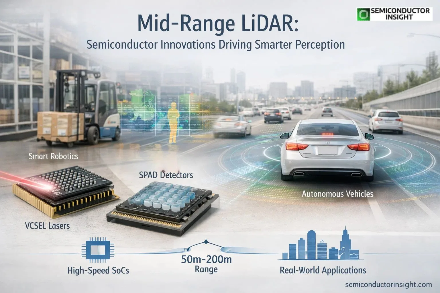
Solid-State Mid-Range LiDAR Market Sensors Led by Advanced Semiconductor Innovations 2026
Imagine navigating a congested warehouse or speeding down a busy highway while an invisible web of laser pulses paints a crystal-clear 3D image of everything around you in real time, including pedestrians, obstructions, and even minute changes in the landscape. That is the silent revolution of mid-range LiDAR, and at its heart are the tiny semiconductor marvels that make it not only feasible but also useful and reasonably priced for everything from smart robotics to self-driving cars.
Mid-range LiDAR systems, typically delivering reliable performance between 50 and 200 meters, strike the perfect balance for dynamic environments where long-range highway scanning meets the precision needed for urban streets or indoor automation.
Semiconductor Lasers Lighting Up Mid-Range Precision
The real magic starts with the light source itself. Edge-emitting lasers (EELs) at 905 nanometers have long powered mid-range LiDAR, offering an economical and compact way to reach up to 200 meters while pairing seamlessly with MEMS mirrors in hybrid designs. Scientific reviews emphasize how EELs deliver solid performance in this sweet spot, balancing cost, size, and output for automotive safety features like adaptive cruise control and emergency braking.
But the spotlight today shines on vertical-cavity surface-emitting lasers, or VCSELs, especially multi-junction versions at 940 nanometers. These semiconductor arrays produce circular, stable beams with excellent temperature stability drifting just 0.07 nanometers per degree Celsius which simplifies receiver filters and boosts overall system reliability.
Recent innovations like antireflective VCSELs push power density higher while keeping divergence low, making them ideal for solid-state mid-range setups that ditch mechanical parts entirely.
SPAD Detectors Capturing Every Critical Photon
- On the receiving end, single-photon avalanche diodes (SPADs) fabricated in standard CMOS processes have transformed what’s possible.
- Back-illuminated SPAD arrays, for instance, deliver a 2x increase in range and 10x boost in photon sensitivity compared to earlier generations, as seen in high-resolution sensors like Ouster’s OS1.
- This mid-range workhorse achieves 90 meters at 10% reflectivity (and up to 200 meters maximum), with 128 vertical channels generating up to 5.2 million points per second.
- The L3 processing chip inside packs 125 million transistors and 21.47 Gmacs of onboard signal crunching, all while maintaining an impressive mean time to failure of at least 250,000 hours.
- These CMOS-integrated detectors operate efficiently across temperatures from -40°C to 60°C, shrugging off shock, vibration, and harsh weather exactly what real-world mid-range applications demand.
Take a Quick Glance at Our In-Depth Analysis Report: https://semiconductorinsight.com/report/mid-range-lidar-market/
High-Speed SoCs Turning Pulses into Smart Decisions
Raw data is useless without lightning-fast processing, and that’s where dedicated LiDAR processor SoCs shine. Next Semiconductor’s NXLR1, unveiled in late 2025, integrates 12 channels of 16-bit analog-to-digital converters sampling at up to 2 billion samples per second each.
With proprietary full-waveform capture built right in, the chip handles laser firing, digitizes complete pulse returns, and delivers curated metadata over high-speed links all while slashing power consumption and costs by 10x compared to older FPGA-based boards. This kind of monolithic semiconductor integration reduces the workload on downstream AI processors, making mid-range LiDAR practical for advanced driver-assistance systems and industrial automation alike. It represents the shift toward chipset-level designs where semiconductors aren’t just components they’re the entire intelligent core.
Mid-Range LiDAR Proving Its Worth in Real Deployments
These advances aren’t stuck in labs. Ouster’s OS1, for example, powers autonomous agricultural tractors that let a single operator oversee an entire fleet with zero downtime, boosting farm productivity through precise 3D mapping and obstacle avoidance. In robotics, the same sensor equips self-charging drones that monitor snow distribution at ski resorts worldwide, extending seasons and enhancing avalanche safety.
Even UK rail networks use mid-range LiDAR for crowd analytics and proactive station management, delivering GDPR-compliant insights without invading privacy. Government-backed studies from the U.S. Department of Transportation highlight how falling production costs thanks to semiconductor scaling have made LiDAR viable for infrastructure monitoring, traffic analysis, and microscopic vehicle tracking in real time.
Semiconductor Innovation Charting the Path Forward
As CMOS processes refine SPADs, VCSEL arrays gain more junctions, and SoCs pack ever-more intelligence onto single chips, mid-range LiDAR is evolving from a high-end luxury to an everyday enabler. The focus remains on tighter integration, lower power, and higher resolution all while keeping systems rugged enough for the real world.
Whether it’s keeping autonomous shuttles safe on city streets or helping robots navigate warehouses, these semiconductor breakthroughs are quietly building a more perceptive, responsive future.
The best part? The technology keeps getting smaller, smarter, and more accessible with every new chip iteration.

Comments (0)