

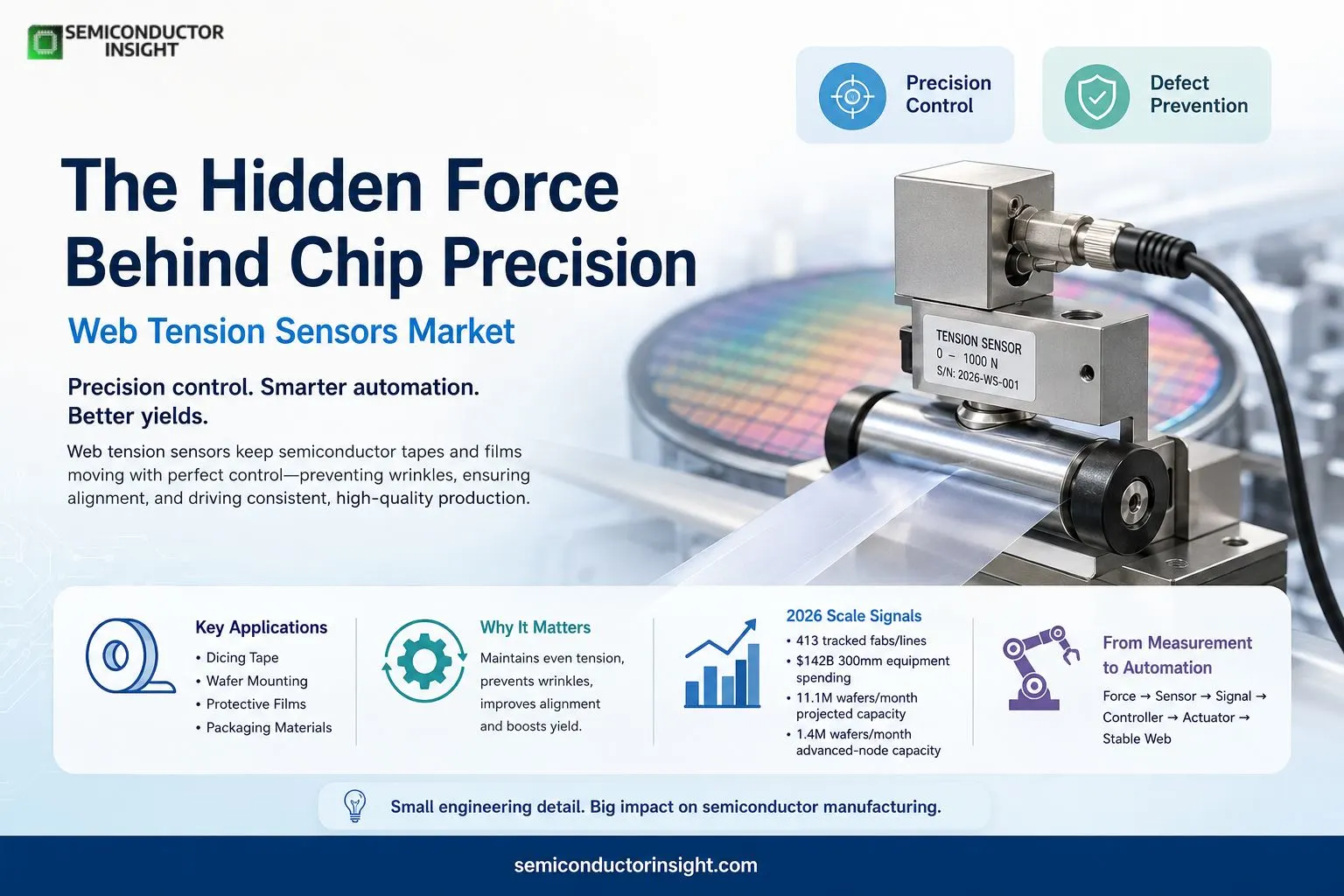
Load Cell vs. Other Sensing Technologies for Web Tension Sensors Control in Semiconductor Processing
Web tension sensors are not typically the first technology associated with semiconductors. Processors, lithography systems, deposition tools and inspection equipment attract far more attention. Yet semiconductor manufacturing also depends on a less visible layer of films, tapes, foils, liners and flexible materials that must move through production equipment without stretching, wrinkling, drifting or losing alignment.
- This becomes particularly important in wafer mounting, dicing tape, protective films and other roll-fed processes.
- Semiconductor Equipment Corporation notes that wafer-mounting systems must maintain tape tension evenly to prevent wrinkles and preserve accurate positioning during application.
- The result is an interesting opportunity for web tension sensors: they sit at the intersection of mechanical precision, automation and material handling.
A sensor that watches what the machine cannot see
The basic principle is straightforward. A moving web passes around a sensing roller, and the force generated by that material is measured by a load cell or tension transducer. The measurement is then fed into a controller, which adjusts a brake, clutch, motor or drive.
Unwind → Tension sensing → Processing / coating / laminating → Alignment → Rewind
In a closed-loop arrangement, the sensor is therefore not merely reporting a measurement. It becomes part of the machine’s feedback system. ABB, for example, describes web-tension systems designed to maintain constant tension during acceleration and deceleration, while its load-cell portfolio spans nominal force ranges from 0.1 kN to 100 kN, depending on configuration.
Semiconductor tapes make tension surprisingly important
- One of the clearest semiconductor-specific applications is wafer dicing tape. These adhesive films are supplied in rolls and must be unwound, positioned and laminated onto frames with high dimensional consistency.
- Patent literature on semiconductor processing tape illustrates why tension cannot be treated as a minor machine parameter.
- Excessive or poorly controlled tension can contribute to wrinkles, dimensional deformation and downstream die-handling problems.
- One disclosed dicing/die-bonding film process specifies winding tension between 20 and 100 N/m, with a preferred range of 30-80 N/m.
- That narrow operating window shows why tension measurement can become a quality-control variable rather than simply a mechanical setting.
The 300mm expansion adds another layer of relevance
The semiconductor industry’s continued investment in larger wafer production provides the broader manufacturing context. SEMI’s latest 300mm outlook tracks 413 fabs and production lines worldwide, while global 300mm front-end equipment spending is projected to reach a record $142 billion in 2026.
SEMI also projects global semiconductor capacity to reach 11.1 million wafers per month by 2028, with advanced 7nm-and-below capacity reaching 1.4 million wafers per month.
More production capacity does not automatically translate into direct sensor demand, but it increases the number of automated material-handling operations where repeatability and process monitoring matter.
You Can Freely Surf Our Latest Updated Report Here: https://semiconductorinsight.com/report/web-tension-sensors-market/
Why closed-loop control is gaining attention?
- Traditional machines can operate using predetermined speed and torque settings. The weakness is that material behaviour changes as roll diameter, elasticity, thickness and surface characteristics change.
- A closed-loop system instead follows the actual condition of the web.
Measured tension → Controller compares target → Drive/brake correction → Web responds → Sensor measures again
- Nexen describes load-cell-based web controls with claimed accuracy of 1-2%, compared with roughly 8-10% for its open-loop diameter-compensation approach.
- For precision film processing, that feedback architecture can reduce the dependence on fixed machine settings.
The sensor is becoming part of the quality system
The most interesting development is the movement from isolated measurement toward process intelligence. A modern tension sensor can provide continuous information that can be combined with line speed, roll diameter, motor load, web position and production recipes.
This creates opportunities for:
Real-time tension monitoring → abnormality detection → automatic correction → defect prevention → production traceability
Research into roll-to-roll manufacturing has also examined nonuniform web tension, particularly because uneven tension can affect flexible and printed electronic production.
Where the next applications are emerging?
The technology’s addressable application base extends beyond semiconductor wafer tape. Similar tension-control principles are used across thin-film processing, flexible electronics, battery materials, specialty films, coating, and laminating, slitting and precision converting.
That crossover is important. Semiconductor manufacturers increasingly operate alongside advanced packaging, display, battery and flexible-electronics supply chains, where roll-to-roll handling is already highly automated. Sensor suppliers that can deliver low-drift measurement, clean mechanical integration and rapid feedback can therefore participate across several precision-manufacturing ecosystems.
2026 visual concepts for the blog
- Inside a Web Tension Control Loop
Roll → Sensor Roller → Process Zone → Drive → Rewind → Feedback - Semiconductor Film Precision Map
Dicing Tape → Wafer Mounting → Protective Film → Packaging Materials → Inspection - 2026 Semiconductor Scale Signals
413 tracked fabs/lines | $142B 300mm equipment spending | 11.1M wafers/month projected capacity | 1.4M wafers/month advanced-node capacity - From Measurement to Automation
Force → Sensor → Signal → Controller → Actuator → Stable Web
Web Tension Sensors Market is therefore best understood not as an isolated sensor category, but as a precision-enabling technology within automated material handling. As semiconductor production becomes faster, more automated and increasingly dependent on thin functional films and tapes, controlling the force applied to those materials becomes a small engineering detail with potentially large consequences for process consistency.

Comments (0)