Lead Frame Market Evolution: From Traditional Packaging to High-Performance Applications
Lead frames are frequently disregarded in the semiconductor value chain in favor of cutting-edge lithography, exclusive IP blocks, and sophisticated dies. Yet for all the breakthroughs in chip performance, lead frames remain a fundamental structural enabler supporting electrical connectivity, thermal management, mechanical stability, and cost-efficient packaging at scale.
As the global semiconductor industry adapts to surging demand across automotive, mobile, IoT, and industrial sectors, Lead Frame Market has emerged as a critical yet highly specialized segment. It is a market driven not by whimsy but by necessity: without robust lead frame solutions, chips cannot reliably serve in demanding real-world environments.
What Is a Lead Frame and Why It Matters Now More Than Ever?
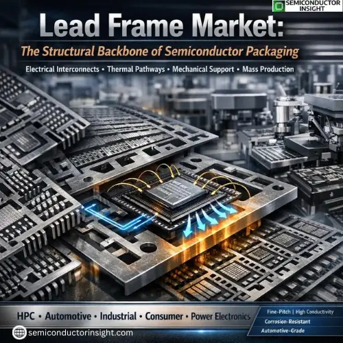
At its core, a lead frame is the metallic skeleton inside a semiconductor package that connects the silicon die to the external world. It provides pathways for electrical signals, mechanical support for the chip, and pathways for heat dissipation all while conforming to the chip’s form factor and required performance characteristics.
Historically, lead frames were simple stamped metals. Today, they are precision-engineered components, designed to accommodate:
- High-frequency signal integrity
- Multi-pin fine pitch requirements
- Thermal conductivity critical to power devices
- Miniaturization in surface-mount technology (SMT)
This transition from commodity metal piece to engineered solution illustrates why the lead frame segment has shifted from a cost centre to a strategic performance lever within packaging technologies.
Material Innovation Considered to be the Shift toward Performance Optimization
One of the biggest recent shifts in the lead frame market is the diversification of materials beyond traditional copper and alloys. Today’s lead frames increasingly incorporate:
- Copper alloys with optimized conductivity and mechanical strength
- Copper plated with silver or nickel for enhanced corrosion resistance
- High-temperature alloys designed for automotive power electronics
These material innovations directly impact end-use reliability. For example, in automotive electronics where devices must operate at elevated temperatures, withstand vibration, and maintain long lifecycles traditional materials often fall short. The adoption of tailored lead frame alloys is rising sharply, mirroring the broader theme of packaging convergence with performance expectations.
Moreover, advanced surface treatments and coatings are now standard to improve wire bond ability and reduce oxidation a critical attribute for high-volume assembly lines.
For More Detailed Insights You Can Surf Our Latest Report Here:
https://semiconductorinsight.com/report/lead-frame-market/
Technical Challenges Shaping the Market
Modern semiconductor packages are trending toward smaller footprints and higher pin counts. This presents a dual challenge for lead frame design:
- Fine Pitch Precision: As die sizes shrink and I/O counts increase, lead frame geometries must be manufactured with incredible accuracy often requiring sub-micron tolerances that push the limits of stamping and etching technologies.
- Signal Integrity for High-Speed Devices: Chips operating at multi-GHz frequencies are sensitive to trace geometry, impedance, and electromagnetic interference. Lead frames must be engineered to manage these factors, not simply conduct electricity.
These challenges mark a shift from viewing lead frames as passive hardware to viewing them as electrically active contributors to performance. Materials science, microfabrication techniques, and simulation-driven design are now critical differentiators.
Supply Chain Complexity and Geographic Trends
The global semiconductor landscape has underscored the importance of resilient and diversified supply chains. Lead frame manufacturing is no exception it lies at the intersection of raw material sourcing, precision tooling, and high-volume assembly.
Asia remains the geographic hub for lead frame production, particularly in countries with established packaging ecosystems such as Taiwan, China, and Korea. However, geopolitical stressors and national strategies to localize semiconductor capabilities have driven investments in domestic production capacity in the U.S. and Europe.
This shift reflects a broader industry trend: to reduce reliance on a concentrated supply base and improve lead times across critical packaging components.
Sustainability and Manufacturing Efficiency
Environmental factors are increasingly influencing market behavior. Lead frame production is energy-intensive, involving metal stamping, plating, and surface finishing all of which have environmental footprints.
Manufacturers are responding by:
- Reducing waste through precision stamping and recycling processes
- Adopting greener plating chemistries
- Improving energy efficiency in fabrication facilities
Sustainability is no longer a buzzword; it’s a market differentiator. OEMs and tier-1 packaging partners are evaluating suppliers not only on performance and cost but on environmental compliance and carbon footprint.
Lead Frame Market, though not always in the spotlight, is central to semiconductor innovation and reliability. As chips become smaller, faster, and more rugged, the strength of the lead frame architecture directly influences overall device performance.
From automotive electrification to industrial power systems, and from miniaturized consumer devices to high-performance computing, lead frames are quietly enabling next-generation electronics. Their evolution driven by material science, precision engineering, and supply chain resilience will continue to shape the semiconductor industry for years to come.
Comments (0)