

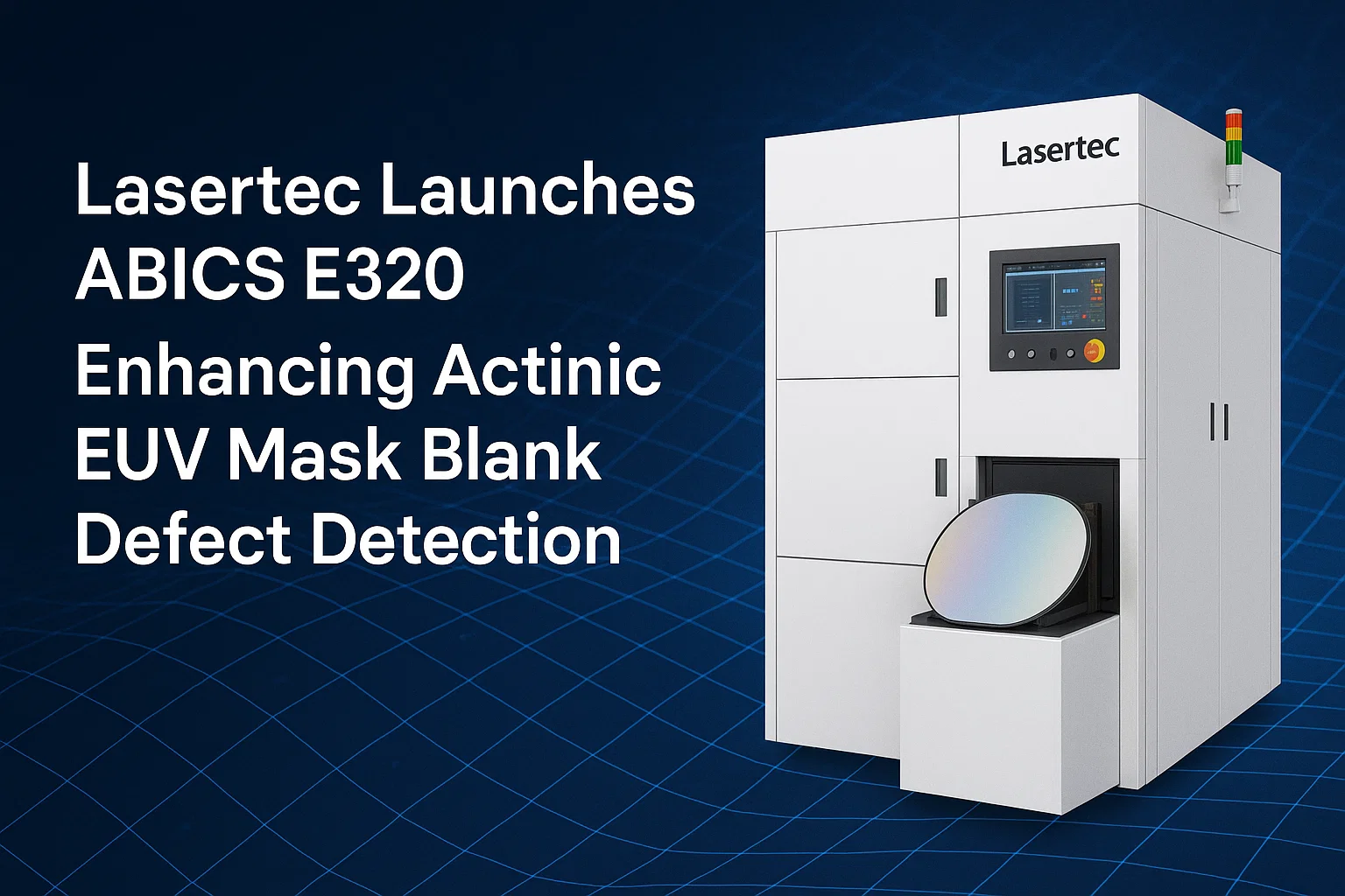
Lasertec Launches ABICS E320, Enhancing Actinic EUV Mask Blank Defect Detection
The semiconductor industry is entering one of its most critical phases in history as the global demand for smaller, faster, and more energy-efficient chips pushes lithography technology to its limits. At the center of this revolution lies Extreme Ultraviolet (EUV) lithography, a technology that allows semiconductor manufacturers to etch features at scales below 5 nanometers. Yet, as promising as EUV lithography is, it also introduces a complex bottleneck EUV mask defect inspection equipment.
These systems play a vital role in ensuring the integrity of photomasks used during chip fabrication. Even microscopic defects in an EUV mask can have massive consequences for yield, device performance, and production costs. This makes inspection equipment indispensable, driving innovation, investment, and international competition.
According to recent industry insights, the global EUV mask defect inspection equipment market was valued at USD 1,502 million in 2024. With the rapid scaling of semiconductor technologies, the market is projected to grow to USD 3,737 million by 2032, registering a CAGR of 14.3%.
Access Your Free Sample Report- EUV Mask Defect Inspection Equipment Market
Why EUV Mask Defect Inspection Is Critical
Before diving into the latest developments, it’s important to understand why defect inspection has become a cornerstone of EUV lithography.
- Extreme Sensitivity at the Nanoscale
At dimensions below 7nm, even the tiniest particle or pattern defect on an EUV mask can translate into significant yield loss. - Mask Blank Defects
Unlike traditional lithography, EUV relies on complex multilayer reflective masks. These masks are sensitive to substrate and multilayer defects that cannot be detected or corrected easily. - Cost of Defects
A single EUV mask can cost several hundred thousand dollars. A flawed mask that escapes detection can multiply losses during mass production. - Inspection at Actinic Wavelength
Because EUV masks operate at a wavelength of 13.5nm, inspection systems must replicate these conditions to accurately detect defects a major technical challenge.
These factors explain why companies like Lasertec, ZEISS, Samsung, and S&S Tech are investing heavily in advanced inspection technologies.
Market Outlook: 2024–2032
The 14.3% CAGR projection for EUV mask defect inspection equipment is underpinned by several drivers:
- Rising Chip Demand
Global demand for AI accelerators, smartphones, high-performance computing, and automotive chips is pushing foundries toward EUV adoption. - Scaling to High-NA EUV
With ASML introducing High-NA EUV systems, mask inspection tools must evolve to handle higher resolution and tighter defect tolerances. - Geopolitical Pressures & Localization
Countries like South Korea, Japan, and China are accelerating investments to reduce reliance on foreign suppliers. - Cost Pressures
The high cost of mask blanks and defect inspection systems increases the importance of yield optimization.
Recent Developments in the Industry
1. Samsung & S&S Tech Push for Localization
One of the most significant shifts is happening in South Korea, where Samsung Electronics is collaborating with S&S Tech to localize EUV mask blank production and inspection capabilities.
- High-Value Equipment Purchases
In late 2024, S&S Tech ordered EUV mask inspection equipment from Japan’s Lasertec, with each machine costing about 7 billion Korean won (USD 30+ million). - Localization Strategy
Samsung is accelerating the acceptance of these machines at S&S Tech’s Yongin factory, aiming to reduce dependence on Japanese suppliers such as Hoya for mask blanks.
This move reflects a broader strategy in the semiconductor industry to diversify supply chains and build domestic ecosystems for critical tools.
2. Lasertec Unveils the ABICS E320 System
Japan’s Lasertec Corporation, a global leader in mask inspection technology, continues to dominate with new product launches.
- ABICS E320
Introduced in late 2024, the ABICS E320 is a next-generation actinic mask blank inspection system. It improves defect detection accuracy for EUV mask blanks, which is critical as foundries scale to advanced nodes. - Defect Management Focus
The system provides enhanced resolution, better review capabilities, and supports tighter defect thresholds required by high-NA EUV lithography.
Lasertec’s consistent innovation has helped it maintain a near-monopoly in this niche, though competitors are beginning to emerge.
Download Sample Report PDF- EUV Mask Defect Inspection Equipment Market
3. ZEISS Upgrades to AIMS® EUV 3.0
Optics giant ZEISS is enhancing its inspection offerings with the AIMS EUV 3.0 system.
- Scanner Emulation
This tool is designed to emulate the conditions of EUV scanners more accurately, particularly mask-side numerical aperture and illumination schemes. - High-NA Readiness
The upgraded tool is optimized for next-generation EUV scanners, ensuring compatibility with sub-3nm nodes. - Customer Integration
ZEISS’s systems are increasingly being adopted by leading foundries to verify the printability of mask defects.
4. Investment Surge: ESOL’s 74 Billion Won Raise
Korean firm ESOL raised around 74 billion won (USD 54 million) in funding to accelerate its development of next-generation EUV technologies.
- Inspection Equipment R&D
The funding is partly directed at developing defect detection and inspection solutions for EUV mask blanks. - Domestic Competition
ESOL’s push highlights growing competition in South Korea’s ecosystem as local players challenge Japanese dominance.
5. China’s Strategic Push into EUV Ecosystem
China, facing export restrictions on EUV tools, is stepping up research into EUV light sources, mask blanks, and inspection equipment.
- Former ASML Scientist Leads Effort
Lin Nan, a former ASML senior scientist, is spearheading new EUV research in China, including inspection technologies that could complement domestic EUV lithography efforts. - AI-Powered Detection
Chinese researchers are also experimenting with deep learning algorithms to detect mask defects, reducing reliance on hardware-based solutions.
While still behind in terms of equipment capability, China’s R&D efforts signal a long-term commitment to self-sufficiency.
Key Industry Trends
1. Rising Cost of Equipment
EUV mask defect inspection machines are among the most expensive tools in a fab. Prices often exceed USD 30 million per unit, creating barriers to entry but also guaranteeing strong demand among top chipmakers.
2. Shift to High-NA EUV
The introduction of High-NA EUV scanners (0.55 NA) will require inspection tools that can handle even smaller defect sizes and more complex illumination conditions.
3. AI & Machine Learning in Defect Detection
AI-based defect classification and pattern recognition are emerging as complementary solutions, reducing reliance on brute-force optical inspection.
4. Localization and Supply Chain Diversification
Countries are racing to establish domestic inspection equipment ecosystems, driven by geopolitical risks and export restrictions.
5. Integration with Mask Repair Tools
Inspection systems are increasingly integrated with mask repair technologies, enabling a closed-loop defect management workflow.
Challenges Facing the Industry
- Technical Complexity
Inspecting at 13.5nm actinic wavelength requires advanced optics, high-power light sources, and precision engineering. - High Cost of Development
With limited suppliers, R&D costs are massive, restricting entry to only a handful of companies. - Supply Chain Dependencies
Heavy reliance on Japanese suppliers like Lasertec and Hoya raises risks for other countries. - Scalability for High-NA
The move to High-NA EUV presents new inspection challenges that current tools are only beginning to address.
Regional Landscape
- Japan: Home to Lasertec, the current leader in EUV mask inspection equipment.
- South Korea: Samsung and S&S Tech are driving localization efforts and investments.
- United States: Collaborates with ASML and ZEISS on integrating EUV inspection into advanced fabs.
- China: Racing to develop domestic inspection technology under tight export restrictions.
Click Here To Download Full Sample Report- EUV Mask Defect Inspection Equipment Market
Future Outlook (2025–2032)
The next decade will be transformative for the EUV mask defect inspection equipment market. By 2032:
- Market Size: Expected to exceed USD 3.7 billion.
- High-NA Adoption: Inspection tools must evolve to support sub-2nm nodes.
- AI Integration: Hybrid hardware-software solutions will dominate.
- New Entrants: Start-ups and research institutes may challenge Lasertec’s dominance.
- Localization: Countries like South Korea and China will strengthen domestic supply chains.
With the market projected to grow at a CAGR of 14.3% and reach USD 3,737 million by 2032, EUV mask defect inspection equipment is set to remain a linchpin of global chipmaking.

Comments (0)