

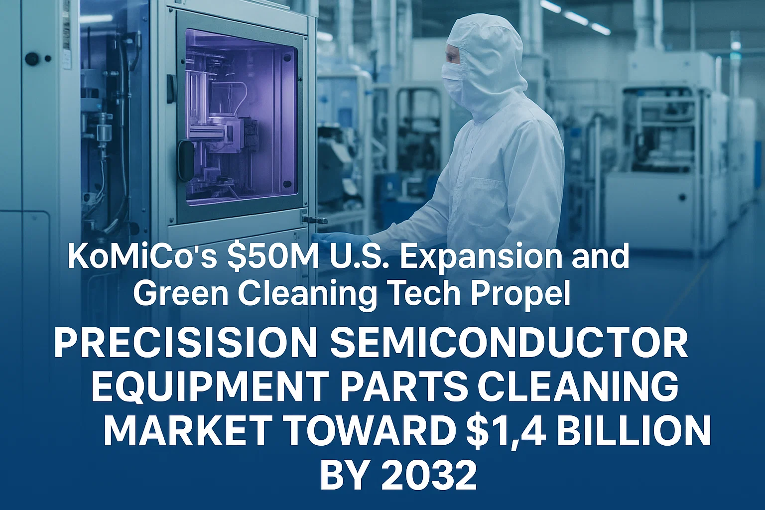
KoMiCo’s $50M U.S. Expansion and Green Cleaning Tech Propel Precision Semiconductor Equipment Parts Cleaning Market Toward $1.4 Billion by 2032
In the fast-paced world of semiconductor fabrication, where transistors are now measured in nanometers and yield losses can cost millions, the humble act of cleaning becomes one of the most critical processes of all. Every piece of wafer-processing equipment from etchers and deposition chambers to CMP tools relies on precisely engineered parts. Over time, those parts accumulate residues, particles, and chemical films. Precision semiconductor equipment parts cleaning ensures that these components can be safely reintroduced into production without compromising yield or performance.
According to industry data, the Precision Semiconductor Equipment Parts Cleaning Market was valued at USD 869 million in 2024 and is projected to reach USD 1,427 million by 2032, growing at a CAGR of 7.5% during the forecast period. This growth reflects not only the swelling capacity of fabs worldwide but also rising expectations for environmental compliance, reduced downtime, and cutting-edge cleaning technologies.
Access Your Free Sample Report- Precision Semiconductor Equipment Parts Cleaning Market
Why Cleaning Matters More Than Ever
Semiconductor fabrication plants (fabs) are cleaner than hospital operating rooms, yet contamination remains an ever-present threat. Wafer process equipment operates under extreme conditions plasma, reactive gases, high temperatures and even trace contamination on tool components can cascade into lower yields or catastrophic defects.
Precision parts cleaning has three core functions:
- Removal of contamination (particles, metals, polymers, and chemical films).
- Extension of component life by removing corrosive or abrasive deposits.
- Maintaining process stability and yield, especially at leading-edge nodes (e.g., 3 nm and below).
These objectives explain why companies such as Applied Materials, Lam Research, Tokyo Electron, and specialized service providers (like KoMiCo, Entegris, and others) invest heavily in cleaning technologies and service facilities.
Recent Developments: A Sector in Motion
1. New Facilities in Strategic Locations
One of the clearest signs of industry momentum is the opening of new service centers. KoMiCo’s new $50 million facility in Mesa, Arizona, announced in August 2024, represents a significant milestone. The plant will provide precision cleaning, coating, and refurbishment services for critical semiconductor equipment parts. Its location reflects the “onshoring” trend spurred by the U.S. CHIPS and Science Act, which is encouraging domestic supply chains to support new fabs being built by TSMC, Intel, and Samsung in the U.S.
KoMiCo’s expansion mirrors a larger shift: moving parts cleaning and refurbishment closer to the fabs themselves. This approach minimizes logistics time, reduces risk during transport, and allows tighter integration with fab maintenance schedules.
2. Rising Demand for Wafer-Cleaning Tools and Services
While wafer cleaning itself is a separate market, it directly influences parts cleaning demand. Companies like ACM Research have posted strong revenue growth in China for advanced wafer cleaning tools, signaling a broader trend of investment in contamination control technologies. As wafer cleaning processes evolve particularly with wet benches, megasonic cleaning, and plasma cleans the components of these tools also experience new types of wear and contamination. This, in turn, drives demand for more sophisticated parts cleaning and coating services.
3. Export Controls and Supply Chain Diversification
Geopolitical shifts have introduced a new wrinkle. The U.S. export controls implemented in 2023–2025 affect not only the sale of advanced lithography and etching equipment to China but also the ecosystem of services around them. Companies providing precision cleaning services for equipment deployed in restricted markets must now navigate licensing and compliance regimes.
This is driving localization of parts cleaning facilities within China and other Asian markets. Chinese fabs are rapidly developing domestic service providers to ensure uninterrupted maintenance of their equipment. Meanwhile, U.S. and European providers are expanding in North America to serve the booming domestic fab buildout.
4. In-Situ Cleaning and Reduced Downtime
Another noteworthy trend is the development of “in-situ” cleaning techniques. Rather than fully removing components from process chambers and sending them out for cleaning, new tools allow cleaning cycles to run while parts remain installed. Plasma or laser-based in-situ cleans can dramatically reduce downtime and maintenance intervals. While this doesn’t eliminate the need for off-tool precision cleaning entirely, it does change the frequency and scope of the work.
Leading fabs are experimenting with hybrid approaches extending the period between full part replacements or cleanings but performing more frequent light cleans inside the chamber. This trend creates both challenges and opportunities for parts cleaning service providers, who must adapt to new cleaning chemistries and shorter turnaround expectations.
5. Environmentally Safer Chemistries and Waste Reduction
Environmental stewardship has emerged as a major theme across the semiconductor ecosystem. Cleaning processes consume vast amounts of ultrapure water and chemicals. Regulators are increasingly scrutinizing hazardous materials such as perfluoroalkyl substances (PFAS) and solvent waste streams. As a result, service providers are shifting toward closed-loop water systems, supercritical CO₂ cleaning, and plasma-based dry cleaning to minimize effluents.
The shift away from legacy solvent-intensive methods not only benefits the environment but can also improve process repeatability and reduce micro-scratching or etch damage to delicate surfaces.
6. Coatings and Surface Engineering
Modern parts cleaning services don’t simply clean they also apply protective coatings to extend component life and improve performance. Coatings such as yttrium oxide (Y₂O₃) or advanced ceramic composites provide resistance to plasma erosion and chemical attack. As equipment cycles get more aggressive at smaller nodes, the interplay between cleaning and coating becomes a key differentiator for service providers.
Market Size and Growth Drivers
With the market projected to grow from USD 869 million in 2024 to USD 1,427 million by 2032, several factors underpin this steady 7.5% CAGR:
- Explosion of fab capacity worldwide – Driven by AI, automotive chips, and geopolitical incentives, more fabs mean more tools, which mean more parts to clean.
- Increasing complexity of process equipment – As deposition, etching, and lithography become more sophisticated, parts accumulate more complex contamination profiles.
- Shorter maintenance cycles – Leading-edge nodes demand ultra-clean conditions, necessitating more frequent cleaning.
- Regional diversification – U.S., Europe, and Southeast Asia are all building fabs, requiring local cleaning support.
- Sustainability pressures – Push for green manufacturing leads to investment in modern cleaning processes and facilities.
Breakdown of the Market by Service Type
- Wet Chemical Cleaning – Still the dominant method, using acids, bases, and solvents in combination with ultrasonic or megasonic agitation.
- Plasma / Dry Cleaning – Gaining ground due to environmental benefits and compatibility with delicate coatings.
- Supercritical Fluid Cleaning – Uses CO₂ under pressure to penetrate crevices and remove contaminants without liquid residue.
- Coating & Refurbishment – Applying new protective layers after cleaning to extend part lifespan.
- Analytical Services – Metrology, particle analysis, and surface inspection to validate cleanliness.
Download Sample Report PDF- Precision Semiconductor Equipment Parts Cleaning Market
Key Players and Their Strategies
While many parts cleaning operations are carried out in-house or by niche providers, several names dominate:
- KoMiCo – Expanding globally with coating and cleaning facilities.
- Entegris (via its Advanced Materials Handling division) – Supplies contamination control and cleaning solutions.
- Lam Research & Applied Materials (service arms) – Offer in-house refurbishment and cleaning for their installed base.
- Regional Specialists – In Taiwan, Korea, China, and Europe, numerous smaller firms handle localized cleaning for major fabs.
Each is differentiating through faster turnaround times, advanced coatings, analytical services, and compliance with environmental regulations.
Technological Innovations to Watch
Automated Robotic Cleaning Cells
Robotic systems are increasingly used to handle heavy, delicate, or hazardous parts during the cleaning process, reducing the risk of contamination and human error.
Data-Driven Maintenance
IoT and digital twins allow fabs to predict when a component needs cleaning. By scheduling cleaning more precisely, fabs can reduce downtime and avoid unnecessary servicing.
Next-Generation Coatings
Companies are experimenting with nanocomposite coatings, which combine ceramic hardness with polymer flexibility to reduce flaking and extend life between cleans.
Closed-Loop Chemical Systems
Recirculating chemicals with in-line filtration minimizes waste and cost while maintaining cleaning performance.
Environmental and Regulatory Pressures
The semiconductor industry is under growing pressure to address its water, energy, and chemical footprints. Precision parts cleaning sits squarely in the crosshairs because it involves:
- High volumes of ultrapure water (UPW).
- Use of acids (HF, HCl, HNO₃) and solvents.
- Disposal or recycling of hazardous waste.
Regulators in the U.S., EU, and Asia are introducing tighter standards for effluents, chemical inventory reporting, and PFAS usage. Companies that can demonstrate greener cleaning methods gain a competitive edge with both regulators and customers.
Regional Outlook
North America
With TSMC, Intel, and Samsung investing billions in U.S. fabs, local supply chains are blossoming. KoMiCo’s Arizona facility exemplifies how parts cleaning is following fab investment.
Asia-Pacific
Still the center of gravity for semiconductor manufacturing, APAC boasts the largest installed base of cleaning and coating service providers. Localization in China is accelerating due to export restrictions.
Europe
New fabs from Intel and TSMC in Germany and elsewhere will require regional parts cleaning hubs. EU environmental regulations will likely push for greener processes.
Challenges Facing the Industry
- Talent Shortage – Specialized chemists, materials engineers, and equipment technicians are in high demand.
- Capital Costs – Setting up advanced cleaning lines with robotics, supercritical systems, and water recycling is expensive.
- Rapid Technology Change – As tool designs evolve, cleaning providers must continually adjust methods.
- Regulatory Complexity – Export controls, environmental regulations, and customer audit requirements create compliance overhead.
Opportunities Ahead
Despite challenges, the precision semiconductor equipment parts cleaning market is brimming with opportunities:
- Integrated Service Packages – Cleaning plus coating plus analytics under one roof.
- Green Cleaning Technologies – Differentiation through sustainability.
- Partnerships with OEMs – Co-developing cleaning protocols with equipment manufacturers for new tool generations.
- Expansion in Emerging Markets – Serving new fabs in India, Vietnam, and the Middle East.
Case Study: KoMiCo’s Mesa Facility
KoMiCo’s new Arizona facility represents a template for the future. By locating near new fabs, it can:
- Offer rapid turnaround for part cleaning and coating.
- Provide on-site engineering support to adjust cleaning processes to specific tool revisions.
- Demonstrate compliance with local environmental regulations using advanced wastewater treatment.
- Expand R&D in coatings and cleaning chemistries in collaboration with U.S. customers.
This model is likely to be replicated by other service providers as regional fab networks develop.
The Role of Coatings in Extending Component Lifespan
Protective coatings are integral to the economics of semiconductor equipment maintenance. They:
- Shield metal surfaces from plasma and chemicals.
- Reduce particle generation.
- Allow more cleaning cycles before a part must be scrapped.
Developments in deposition methods like thermal spray, physical vapor deposition (PVD), or atomic layer deposition (ALD) are creating coatings with finer control and better adhesion, improving performance and reducing flaking.
Click Here To Download Full Sample Report- Precision Semiconductor Equipment Parts Cleaning Market
Digital Transformation of Cleaning Services
A subtle but powerful trend is the digitization of cleaning workflows:
- Traceability – Each part has a digital history of cleans, coatings, inspections.
- AI-Based Scheduling – Predictive models anticipate when a part will exceed contamination thresholds.
- Remote Audits – Customers can view cleaning metrics in real time.
This data-driven approach allows service providers to become strategic partners in yield management, not just vendors. With a forecast 7.5% CAGR and a projected USD 1.427 billion market by 2032, parts cleaning is no longer just a maintenance line item it’s a strategic lever for yield, sustainability, and supply-chain resilience.

Comments (0)