
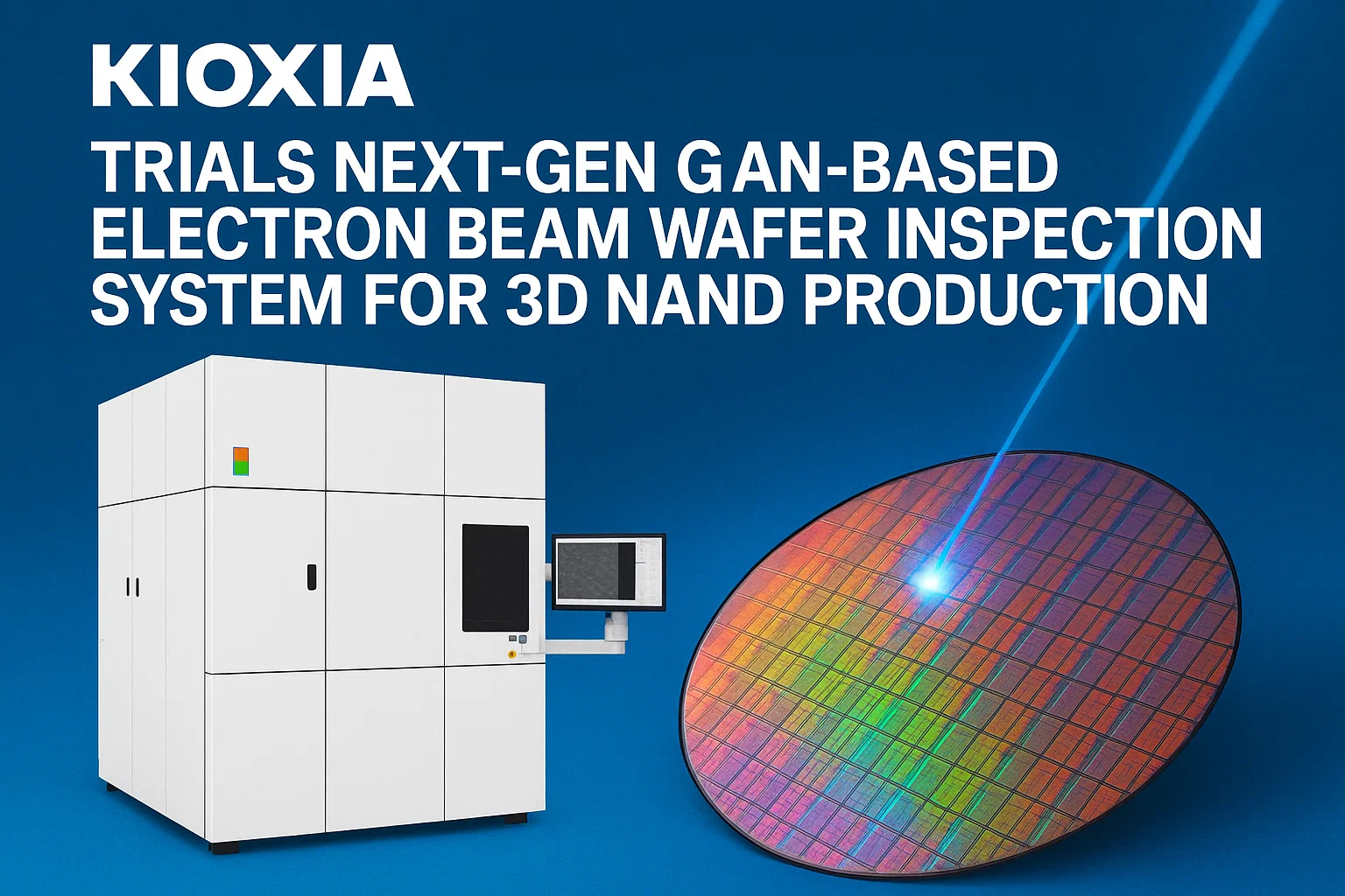
Kioxia Trials Next-Gen GaN-Based Electron Beam Wafer Inspection System for 3D NAND Production
The semiconductor industry is at the forefront of technological evolution, driving advancements in everything from artificial intelligence (AI) to autonomous vehicles, data centers, and next-generation consumer electronics. With every new node transition—moving from 7nm to 5nm, 3nm, and now approaching 2nm and below—the complexity of integrated circuits (ICs) has skyrocketed. This miniaturization trend, coupled with the rise of advanced packaging, 3D NAND architectures, and heterogeneous integration, has amplified the importance of defect inspection and yield management.
Among the numerous inspection technologies available, Electron Beam Wafer Defect Inspection Systems (e-Beam WDI) have emerged as a critical solution for identifying nanoscale defects that optical inspection tools often miss. These systems utilize high-energy electron beams to achieve extremely high resolution, enabling the detection of stochastic defects introduced by advanced lithography processes such as EUV (Extreme Ultraviolet) lithography.
Access Your Free Sample Report- Electron Beam Wafer Defect Inspection System Market
Market Overview
The Electron Beam Wafer Defect Inspection System market has witnessed significant growth in recent years, driven by the increasing complexity of chips and the demand for higher yields. According to the latest projections:
- Market size in 2024: US$642 million
- Expected market size by 2032: US$1.0 billion
- CAGR (2025–2032): 9%
This growth trajectory underscores the pivotal role e-Beam inspection systems will play in future semiconductor manufacturing.
Why Electron Beam Inspection Is Becoming Indispensable
Traditional optical inspection systems, while fast, are limited in resolution. As technology nodes shrink below 5nm, and as EUV lithography introduces stochastic defects, optical systems can no longer capture all the critical defects. Here’s why e-Beam inspection is gaining traction:
1. Shrinking Node Sizes and Advanced Nodes
At advanced technology nodes such as 3nm and 2nm, critical dimensions are so small that line edge roughness, pattern bridging, and stochastic defects become major yield limiters. Optical tools simply cannot provide the necessary resolution to detect these anomalies.
2. EUV Lithography and Stochastic Defects
EUV lithography, essential for sub-7nm nodes, introduces random patterning errors due to the low photon count per feature. These defects—often non-repeating—are extremely difficult to detect with optical systems. Electron beams, however, provide the high-resolution imaging required for effective EUV process control.
3. Advanced Packaging and 3D NAND
As 3D NAND layers increase (moving from 128 to over 500 layers), and with the rise of advanced packaging such as 2.5D interposers and chiplets, new defect modes emerge. e-Beam systems help inspect buried structures, micro-bumps, and TSVs (Through-Silicon Vias) with unmatched accuracy.
Recent Technological Advancements & News Highlights
The past year has seen remarkable innovations in e-Beam wafer inspection systems, addressing historical limitations such as throughput and data handling. Below, we explore some of the most significant developments from leading companies and research groups.
1. Kioxia Iwate Evaluates GaN-Based Photocathode e-Beam System
One of the most groundbreaking developments comes from Kioxia Iwate, which is set to evaluate a novel GaN-based photocathode e-Beam inspection system developed by Photo electron Soul Inc. in collaboration with Nagoya University’s Amano-Honda Laboratory.
Key Features of This System
- GaN-based Photocathode: Provides higher brightness and longer lifetime than traditional photocathodes, improving image clarity and reducing maintenance.
- DSeB (Digital Selective e-Beaming): Enables selective scanning of critical regions, reducing overall scan time while maintaining resolution.
- YCeB (Yield Controlled e-Beaming): Focuses inspection resources on yield-impacting features, optimizing production efficiency.
Impact:
This innovation signals a paradigm shift from e-Beam being used primarily for sampling and R&D to high-volume manufacturing (HVM). For 3D NAND flash memory production, where defect density and complexity are extremely high, these features can significantly improve time-to-yield and reduce cost-per-wafer.
2. PDF Solutions’ High-Throughput Point Scan Technology
PDF Solutions has introduced a point scan e-Beam inspection technique that can inspect over 1 billion hotspots per hour. This advancement addresses one of the biggest drawbacks of traditional e-Beam systems—slow throughput.
How It Works
- Utilizes continuous stage scanning combined with pixel-level defect detection.
- Targets high-risk hotspots identified through AI-driven pattern analysis.
- Eliminates the need for full-field scanning, improving throughput by orders of magnitude.
Why It Matters:
Throughput has always been the Achilles’ heel of e-Beam systems. By adopting selective inspection and AI integration, PDF Solutions’ technology makes e-Beam inspection more viable for inline process monitoring.
Download Sample Report PDF- Electron Beam Wafer Defect Inspection System Market
3. Applied Materials Launches SEMVision™ H20
Applied Materials, a global leader in semiconductor process equipment, has introduced SEMVision™ H20, an advanced defect review system that leverages second-generation cold field emission technology.
Advantages
- Delivers sharper images at lower voltages, ideal for delicate structures at 3nm and below.
- Supports full-stack defect analysis, enabling both logic and memory chip manufacturers to accelerate yield learning.
Industry Impact:
This launch reinforces Applied’s position in the high-end defect inspection market, complementing its Patterning Control portfolio.
4. AI-Driven Defect Classification with Vision Transformers
In June 2025, researchers demonstrated that Vision Transformer (ViT) models can classify wafer defect images captured by Scanning Electron Microscopes (SEM) with over 90% accuracy, using as few as 15 samples per defect class.
Benefits
- Reduces reliance on large labeled datasets, accelerating deployment.
- Improves root cause analysis and reduces engineering time for defect review.
- Paves the way for fully automated defect inspection workflows.
Market Growth and Key Drivers
The e-Beam wafer defect inspection system market is projected to expand from US$642 million in 2024 to US$1.0 billion by 2032, at a CAGR of 6.9%. Several factors are fueling this growth:
1. AI and Machine Learning Integration
Next-generation e-Beam tools incorporate AI for hotspot identification, image enhancement, and defect classification, reducing manual review time.
2. Complexity of Advanced Nodes
As the industry moves toward 2nm and beyond, optical inspection tools struggle to detect stochastic defects, making e-Beam indispensable.
3. Growth of 3D NAND and Advanced Packaging
The vertical scaling of memory chips and heterogeneous integration create new defect types that require high-resolution imaging.
Regional Insights
- Asia-Pacific (APAC):
Dominates the market due to the presence of leading fabs in Taiwan (TSMC), South Korea (Samsung, SK Hynix), and Japan (Kioxia). - North America:
Driven by Intel’s advanced node roadmap and U.S. government initiatives to strengthen domestic semiconductor manufacturing. - Europe:
Focuses on automotive and power electronics, boosting demand for defect inspection in wide-bandgap semiconductor production.
Challenges and Limitations
Despite its advantages, e-Beam inspection faces challenges:
- Throughput Limitations:
Even with point scan and multi-beam approaches, matching optical inspection speed is difficult. - High Cost:
Systems can cost $10–15 million each, restricting adoption among smaller fabs. - Data Management:
Massive image data requires robust storage and analytics infrastructure.
Click Here To Download Full Sample Report- Electron Beam Wafer Defect Inspection System Market
Future Outlook and Opportunities
Looking ahead, e-Beam inspection is expected to move from niche R&D use to mainstream high-volume manufacturing. Key trends include:
- Multi-Beam Systems:
To overcome throughput limitations, vendors are exploring multi-column e-Beam architectures. - AI-Powered Automation:
Automated defect classification will enable real-time decision-making. - Integration with Smart Fabs:
As fabs adopt Industry 4.0 practices, e-Beam tools will feed data into predictive yield models for closed-loop process control.
The semiconductor industry’s relentless pursuit of smaller, faster, and more efficient chips has elevated the importance of precision defect inspection. Electron Beam Wafer Defect Inspection Systems, once limited by throughput, are now undergoing a renaissance thanks to GaN-based photocathodes, point scan technologies, AI-driven analytics, and advanced emission sources.
As the market grows from US$642 million in 2024 to US$1.0 billion by 2032, e-Beam inspection will become a cornerstone of semiconductor manufacturing, ensuring that the next generation of chips meets the world’s ever-increasing performance and reliability demands.

Comments (0)