Market Insights
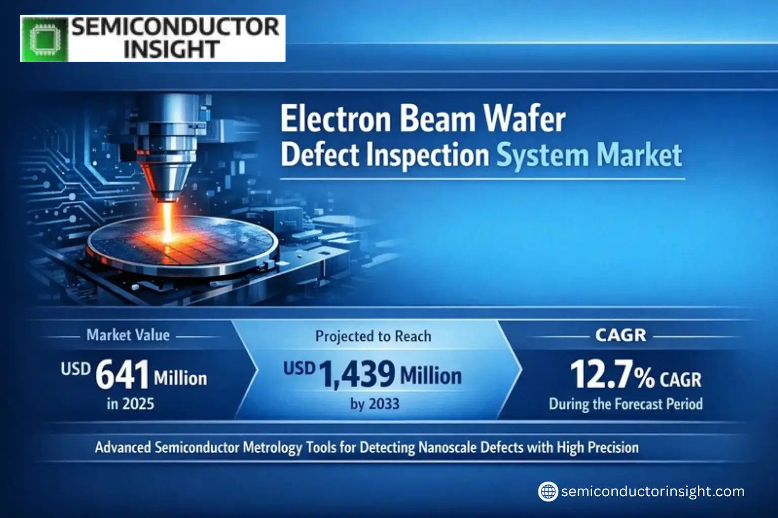
Global Electron Beam Wafer Defect Inspection System Market was valued at USD 641 million in 2025 and is projected to reach USD 1,439 million by 2033, exhibiting a CAGR of 12.7% during the forecast period.
Electron Beam Wafer Defect Inspection Systems are advanced semiconductor metrology tools designed to detect nanoscale defects on wafers with high precision. These systems utilize focused electron beams to scan wafer surfaces, identifying critical defects such as particles, pattern irregularities, and material inconsistencies that impact chip yield. The technology enables sub-nanometer resolution imaging, making it indispensable for cutting-edge semiconductor manufacturing nodes below 10nm.
The market growth is driven by increasing demand for smaller, more powerful semiconductor devices across applications like AI processors, 5G chips, and automotive electronics. As foundries transition to advanced nodes (3nm and below), the need for higher sensitivity defect detection has intensified. Key players like ASML Holding NV and KLA Corporation are investing heavily in multi-beam inspection technologies to address throughput challenges in high-volume manufacturing environments.
MARKET DRIVERS
Growing Demand for Semiconductor Miniaturization
Electron Beam Wafer Defect Inspection System Market is experiencing significant growth due to the rising demand for smaller and more efficient semiconductor components. As chip manufacturers push the limits of Moore’s Law, advanced inspection technologies are required to detect nanometer-scale defects. Global semiconductor industry’s shift toward 5nm and 3nm process technologies has accelerated adoption of electron beam systems.
Increasing Complexity of Semiconductor Manufacturing
With the proliferation of 3D NAND, FinFET, and GAA transistor architectures, wafer inspection has become more challenging. Electron beam systems provide superior resolution compared to optical inspection methods, enabling detection of critical defects in complex multilayer structures. The market is projected to grow at approximately 8-10% annually as foundries upgrade their inspection capabilities.
Additional growth drivers include stringent quality requirements in automotive semiconductors and the expansion of memory chip production capacity across Asia.
MARKET CHALLENGES
High System Costs and Throughput Limitations
While electron beam wafer defect inspection systems offer unparalleled precision, their adoption is constrained by high capital expenditure and relatively slow inspection speeds compared to optical systems. A single advanced e-beam inspection tool can cost USD 5-8 million, creating significant barriers for smaller semiconductor manufacturers.
Other Challenges
Technology Complexity
The operation and maintenance of electron beam systems requires highly skilled personnel, adding to the total cost of ownership. Many fabs struggle with integrating these systems into existing production lines without disrupting yield.
MARKET RESTRAINTS
Economic Uncertainty in Semiconductor Sector
The cyclical nature of the semiconductor industry presents a key restraint for the electron beam wafer defect inspection system market. During periods of reduced capex spending, manufacturers often delay or cancel purchases of high-value inspection equipment. Recent memory market downturns have temporarily slowed adoption rates in some segments.
MARKET OPPORTUNITIES
Expansion in Emerging Semiconductor Applications
Electron Beam Wafer Defect Inspection System Market is poised for growth with the expansion of compound semiconductor manufacturing for 5G, AI, and automotive applications. GaN and SiC wafer producers are increasingly adopting e-beam inspection to maintain quality standards as these materials gain market share.
Electron Beam Wafer Defect Inspection System Market Trends
Rapid Market Growth Fueled by Semiconductor Industry Demands
Global Electron Beam Wafer Defect Inspection System Market was valued at USD 641 million in 2025 and is projected to reach USD 1,439 million by 2033, growing at a CAGR of 12.7%. This growth is driven by increasing complexity in semiconductor devices and stricter quality control requirements in fabrication processes. As chip architectures become more advanced with tighter process windows, the demand for high-sensitivity 2D and 3D imaging solutions intensifies.
Other Trends
Automotive Sector Expansion
The electrification and automation in automobiles is creating substantial demand for wafer-based components used in systems like GPS, ABS, and vehicle control systems. This application segment requires precise defect inspection capabilities to ensure reliability of critical automotive electronics.
Technological Segmentation Driving Product Innovation
The market is segmented by defect detection capability into Less than 1 nm, 1 nm to 10 nm, and More than 10 nm systems. The 1 nm to 10 nm segment currently dominates with over 45% market share as it meets most advanced node requirements. Meanwhile, wafer size segmentation shows 300mm wafers accounting for nearly 60% of the market due to their prevalent use in high-volume semiconductor manufacturing.
Regional Market Dynamics
Asia Pacific leads the market with 58% share, driven by semiconductor manufacturing hubs in China, Japan, South Korea and Taiwan. North America follows with 22% share, supported by advanced R&D facilities and major fabless semiconductor companies demanding cutting-edge inspection capabilities.
Competitive Landscape and Key Players
The market features established players like ASML Holding NV and KLA Corporation alongside emerging competitors such as Wuhan Jingce Electronic Group. These companies are investing heavily in faster, more sensitive inspection systems to meet the demands of next-generation chips requiring advanced defect detection capabilities beyond traditional eBeam systems.
COMPETITIVE LANDSCAPE
Key Industry Players
Technological Innovation Drives Market Leadership in E-Beam Wafer Inspection
The Electron Beam Wafer Defect Inspection System Market is dominated by semiconductor equipment giants with ASML Holding NV and KLA Corporation leading through advanced imaging technologies and AI-powered defect analysis solutions. These market leaders hold over 45% combined market share, leveraging their deep R&D investments and strategic partnerships with leading foundries. Applied Materials and Hitachi High-Tech Corporation follow with strong positions in 3D NAND and logic device inspection segments, particularly for sub-7nm node applications.
Emerging players like TASMIT and Wuhan Jingce Electronic Group are gaining traction in the Chinese semiconductor ecosystem through localized solutions. Niche specialists such as Camtek and Onto Innovation focus on memory wafer inspection, while Japanese firms JEOL and Advantest cater to specialized applications in compound semiconductor and photomask inspection.
List of Key Electron Beam Wafer Defect Inspection System Companies Profiled
- ASML Holding NV
- KLA Corporation
- Applied Materials
- Hitachi High-Tech Corporation
- TASMIT, Inc.
- Wuhan Jingce Electronic Group
- JEOL Ltd.
- Camtek Ltd.
- Onto Innovation
- Advantest Corporation
- Carl Zeiss AG
- NuFlare Technology
- Direct Electron
- Thermo Fisher Scientific
- Intego GmbH
Segment Analysis:
| Segment Category | Sub-Segments | Key Insights |
| By Type |
|
1 nm to 10 nm dominates the market due to:
|
| By Application |
|
300mm Wafer shows strongest growth potential because:
|
| By End User |
|
Foundries lead in adoption owing to:
|
| By Technology Node |
|
Below 7nm segment is gaining traction because:
|
| By Inspection Mode |
|
Multi-Beam technology is emerging as key differentiator:
|
Regional Analysis: Electron Beam Wafer Defect Inspection System Market
Taiwan accounts for the highest electron beam system density globally due to TSMC’s advanced node development. The concentrated ecosystem of IC design houses and OSAT providers creates sustained demand for high-resolution defect inspection across 300mm wafer production lines.
Samsung and SK Hynix drive specialized electron beam adoption for 3D NAND and DRAM production where vertical stacking creates unique defect patterns. The need for layer-by-layer inspection in high-aspect ratio structures makes electron beam indispensable.
Despite export controls, Chinese foundries like SMIC are implementing electron beam systems through domestic suppliers and secondary equipment channels. The focus remains on mature nodes while developing capability for advanced logic and specialty chips.
Japan’s market emphasizes electron beam inspection for power semiconductors and advanced packaging. The strong materials science ecosystem supports unique inspection requirements for gallium nitride and silicon carbide wafers.
North America
North America maintains technology leadership through equipment vendors like Applied Materials and KLA, with strong R&D adoption at Intel and GlobalFoundries. The region shows increasing electron beam usage for advanced packaging inspection including chiplets and heterogeneous integration. Defense applications drive specialized requirements for radiation-hardened chips inspected under classified protocols. Research institutions pioneer in-situ electron beam techniques development for next-generation devices.
Europe
Europe’s electron beam wafer inspection market centers on automotive and industrial semiconductor production with Infineon, STMicroelectronics, and NXP as key adopters. The region emphasizes system customization for analog/mixed-signal chips with large inspection areas. Collaborative research projects under Horizon Europe focus on electron beam metrology standardization for compound semiconductors.
Middle East & Africa
The region is emerging through strategic investments in semiconductor test and packaging facilities in Israel and UAE. Limited front-end production creates niche demand for failure analysis applications rather than inline inspection. Growing academic cooperation with Asian and European institutions builds regional electron beam expertise.
South America
Brazil leads in selective adoption of electron beam systems through government-academia partnerships in microelectronics. The focus remains on educational use and prototype development rather than high-volume manufacturing. Local IC design activities create demand for selective inspection services through regional foundry partners.
Report Scope
This market research report provides a comprehensive analysis of the Electron Beam Wafer Defect Inspection System Market, covering the forecast period 2025–2033. It offers detailed insights into market dynamics, technological advancements, competitive landscape, and key trends shaping the industry.
Key focus areas of the report include:
- Market Overview: The report begins with an overview outlining its current market scenario, key growth indicators, and industry transformation drivers. It discusses macroeconomic factors, demand–supply balance, regulatory landscape, and the strategic role of semiconductors in powering advancements across industries such as automotive, telecommunications, consumer electronics, and industrial automation.
- Market Size & Forecast: Historical data and future projections for revenue, unit shipments, and market value across major regions and segments.
- Segmentation Analysis: Detailed breakdown by product type, technology, application, and end-user industry to identify high-growth segments and investment opportunities.
- Regional Insights: Insights into market performance across North America, Europe, Asia, South America, and Middle East & Africa, including country-level analysis where relevant.
- Competitive Landscape: Profiles of leading market participants, including their product offerings, R&D focus, manufacturing capacity, pricing strategies, and recent developments such as mergers, acquisitions, and partnerships.
- Technology Trends & Innovation: Assessment of emerging technologies, integration of AI/IoT, semiconductor design trends, fabrication techniques, and evolving industry standards.
- Market Drivers & Restraints: Evaluation of factors driving market growth along with challenges, supply chain constraints, regulatory issues, and market-entry barriers.
- Stakeholder Insights: Insights for component suppliers, OEMs, system integrators, investors, and policymakers regarding the evolving ecosystem and strategic opportunities.
Primary and secondary research methods are employed, including interviews with industry experts, data from verified sources, and real-time market intelligence to ensure the accuracy and reliability of the insights presented.
FREQUENTLY ASKED QUESTIONS:
What is the current market size of Electron Beam Wafer Defect Inspection System Market?
-> Electron Beam Wafer Defect Inspection System Market was valued at USD 641 million in 2025 and is projected to reach USD 1,439 million by 2033, exhibiting a CAGR of 12.7% during the forecast period.
What is the growth rate (CAGR) of Electron Beam Wafer Defect Inspection System Market?
-> The market is expected to grow at a CAGR of 12.7% during the forecast period (2025-2033).
Which key companies operate in Electron Beam Wafer Defect Inspection System Market?
-> Key players include ASML Holding NV, KLA Corporation, TASMIT Inc., Applied Materials, Hitachi High-Tech Corporation, Wuhan Jingce Electronic Group, and DJEL.
What are the key growth drivers?
-> Key drivers include increasing semiconductor complexity, demand for faster defect inspection systems, and growth in automotive electrification and automation.
Which region dominates the market?
-> Asia-Pacific leads the market due to strong semiconductor manufacturing presence, while North America and Europe show significant adoption of advanced inspection technologies.
What are the emerging trends?
-> Emerging trends include higher sensitivity in 2D and 3D imaging, faster eBeam inspection systems, and integration with advanced process control solutions.

Get Sample Report PDF for Exclusive Insights
Report Sample Includes
- Table of Contents
- List of Tables & Figures
- Charts, Research Methodology, and more...