

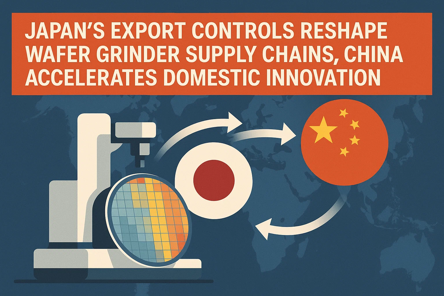
Japan’s Export Controls Reshape Wafer Grinder Supply Chains, China Accelerates Domestic Innovation
The semiconductor industry is in the middle of a historic transformation, and one of the most critical—yet often overlooked—technologies enabling this shift is wafer thinning. Also known as wafer grinding, this process is essential for manufacturing the advanced chips that power everything from smartphones and servers to artificial intelligence accelerators and high-performance computing systems.
In 2024, the global wafer grinder (wafer thinning equipment) market was valued at approximately US$ 951 million. Projections suggest it will grow to US$ 1.6 billion by 2032, representing a compound annual growth rate (CAGR) of 7.7%. This impressive growth trajectory reflects not only rising semiconductor demand but also the structural importance of wafer thinning in advanced packaging technologies.
Access Your Free Sample Report- Wafer Grinder (Wafer Thinning Equipment) Market
Why Wafer Thinning Matters
Traditionally, semiconductor wafers were left relatively thick, making them easier to handle during manufacturing. But as chip technology advanced, packaging requirements changed dramatically. Today, ultra-thin wafers—sometimes just 30–50 microns thick—are essential for:
- 3D chip stacking (e.g., high bandwidth memory or HBM).
- Advanced logic packaging in AI accelerators.
- Mobile devices, where compact size and heat management are critical.
- Automotive electronics, where reliability under stress demands precise wafer thickness control.
Wafer grinders and polishers enable this process by carefully thinning wafers without introducing defects such as cracks or warpage. The rise of chiplet-based architectures and hybrid bonding techniques has made wafer thinning even more critical.
Market Outlook: From $951M to $1.6B
The wafer grinder market’s growth path—$951M in 2024 to $1.6B by 2032—is underpinned by several megatrends:
- AI and HPC Demand: NVIDIA, AMD, and other chipmakers require massive volumes of HBM, which relies on ultra-thin wafers.
- 2nm and Beyond: Foundries like TSMC, Samsung, and Intel are racing to adopt wafer thinning for advanced packaging nodes.
- 3D NAND Expansion: Storage devices with stacked memory layers depend on thinning equipment.
- Mobile & Automotive Growth: IoT, EVs, and smartphones add sustained wafer demand.
- Geopolitics & Localization: Export restrictions and reshoring of semiconductor fabs create new equipment opportunities.
With 7.7% CAGR, the wafer grinder market is growing faster than the broader semiconductor equipment sector, signaling its unique importance.
Recent Developments and Industry News
1. Surge in Demand from AI and HPC
The AI revolution has had a direct impact on wafer thinning equipment demand. NVIDIA’s H100 GPUs and AMD’s MI300 accelerators use stacked HBM memory, which cannot function without ultra-thin wafers. Every additional rack of AI servers being deployed globally represents a ripple effect of demand across the wafer thinning supply chain.
- 2024–2025: Reports from The Register, Digitimes, and TechPowerUp confirm that HBM manufacturers are scrambling to expand capacity, driving up equipment orders.
- This means wafer grinders are not just part of back-end processing—they are now mission-critical for enabling AI-driven economies.
2. Key Equipment Suppliers Expanding
- DISCO Corporation (Japan)
DISCO remains the global leader in wafer thinning and dicing solutions. According to Nikkei Asia, the company recorded record orders in FY2024 due to soaring AI-related demand. It has also expanded its facilities to ensure supply capacity, particularly for HBM-related equipment. - Tokyo Seimitsu (Accretech)
Tokyo Seimitsu has focused on R&D for precision grinders capable of handling wafers under 50 microns. Their tools are becoming increasingly crucial in 3D NAND and HBM production. Analysts from EE Times note that the company is strengthening its position as a challenger to DISCO’s dominance. - Applied Materials & Lam Research
While not direct suppliers of wafer grinders, they are critical players in complementary packaging steps. Applied has been vocal in its quarterly calls about the surge in demand for hybrid bonding and packaging equipment, both of which go hand-in-hand with wafer thinning.
Download Sample Report PDF- Wafer Grinder (Wafer Thinning Equipment) Market
3. Shift Toward Hybrid Bonding and 3D Packaging
As noted by Semiconductor Engineering, hybrid bonding requires wafers to be thinned to extreme levels without surface damage. This has pushed grinder companies to refine technologies to improve flatness, surface integrity, and throughput.
The transition from wire bonding to hybrid bonding in advanced logic and memory packaging could double the demand for wafer thinning equipment in the next decade.
4. Geopolitical Headwinds: Japan’s Export Controls
In 2023–2024, Japan tightened semiconductor equipment export rules, limiting sales of critical tools to China. Since both DISCO and Tokyo Seimitsu are Japanese, these restrictions directly impacted the wafer grinder market.
- Reuters and Bloomberg highlighted that while China remains a large semiconductor market, Japanese companies are increasingly prioritizing supply to allies in the U.S., Taiwan, and South Korea.
- The export controls have accelerated China’s efforts to develop domestic wafer thinning technologies, though catching up with Japanese precision engineering will take time.
Technology Trends Driving Wafer Grinding
Ultra-Thin Wafers (<50 Microns)
For HBM and 3D integration, wafers need to be almost as thin as a human hair. Achieving this while preventing mechanical stress or warping requires advanced grinding and polishing techniques.
Automation and AI Integration
Modern wafer grinders are incorporating AI-based monitoring to detect micro-cracks or surface deviations during the thinning process. This reduces yield loss in high-value chips.
Eco-Friendly Processing
Water usage and slurry disposal are becoming environmental concerns. Equipment makers are investing in eco-efficient slurry recycling systems to align with ESG goals.
Competitive Landscape
- DISCO Corporation – Market leader with strong dominance in wafer thinning and dicing.
- Tokyo Seimitsu (Accretech) – Rising competitor with advanced grinders for ultra-thin wafers.
- Chinese Entrants – Emerging but facing technological gaps due to export controls.
- Applied Materials / Lam Research – Complementary players in packaging ecosystems.
The Japanese duopoly of DISCO and Tokyo Seimitsu is expected to continue dominating, but geopolitical shifts could reshape competition.
Challenges Facing the Industry
- Geopolitical Tensions – Export bans risk fragmenting supply chains.
- Technical Complexity – Thinning wafers below 30 microns without yield loss remains challenging.
- High Costs – Advanced grinders are extremely capital-intensive.
- China’s Push for Independence – Long-term competitive threat if domestic innovation succeeds.
Click Here To Download Full Sample Report- Wafer Grinder (Wafer Thinning Equipment) Market
The Road Ahead: 2025–2032
Looking forward, wafer grinding equipment will continue to evolve alongside semiconductor packaging innovations. Expect:
- Integration with Hybrid Bonding Lines: Fully automated wafer thinning + bonding ecosystems.
- More Suppliers: Non-Japanese companies may attempt entry due to geopolitical risks.
- Regional Capacity Growth: U.S. CHIPS Act and EU Chips Act could spur local demand for grinders.
- AI-Driven QC Systems: Equipment increasingly reliant on real-time defect detection powered by machine learning.
The projected US$ 1.6 billion market by 2032 underscores how wafer thinning will remain a hidden but vital enabler of technological progress.

Comments (0)