
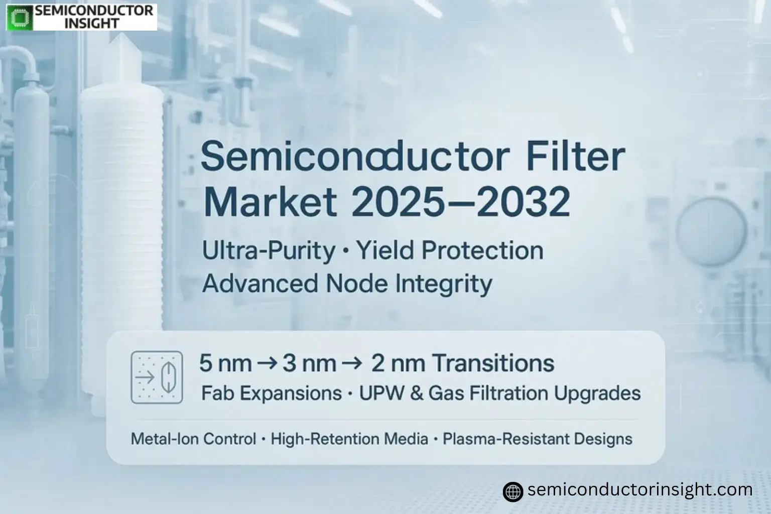
Inside the Semiconductor Filter Market: The Hidden Engine behind High-Yield Manufacturing
In the semiconductor world, contamination is the enemy. A speck of organic residue, a stray metallic ion, or an unseen airborne particle can ruin a wafer worth thousands of dollars or disrupt an entire production run.
Semiconductor filters may not be visible to the end user, but they sit at the front line of yield protection. As chip geometries shrink and fabs push toward more complex nodes, these filters have become mission-critical assets rather than simple consumables.
A Market Focused on Accuracy Rather than Volume
Unlike many materials used in chip making, semiconductor filters aren’t demanded in massive numbers they’re demanded in precise performance tiers. Every filter is judged on:
- Retention efficiency at sub-micron and sub-nanometre scales
- Extractable contaminants, which must stay close to zero
- Thermal and chemical resistance, especially for acids, solvents, and CMP slurries
- Process compatibility across EUV lithography, PECVD, ALD, etching, and ultrapure water loops
This is a market defined by quality control, process integrity, and lifecycle reliability key themes driving procurement decisions at leading fabs in the U.S., Taiwan, Korea, Japan, and Europe.
Why the Market Is Expanding Faster Than Most Fab Supplies
The Semiconductor Filter Market is growing at a pace that mirrors broader industry transitions. Several forces are aligning at once:
- The Move toward Advanced Nodes
As chipmakers push into 5 nm, 3 nm, and exploratory 2 nm territory, defect tolerances shrink dramatically. Filters now must capture particles so small that conventional testing methods are being rewritten. This shift is pushing premium, high-retention filters into wider use, especially in:
- EUV photolithography lines
- High-purity gas delivery
- Chemical blending stations
- The Fab Capacity Boom
Governments and foundries worldwide are building or expanding manufacturing sites from Arizona and Ohio to Osaka, Dresden, Pyeongtaek, and Singapore. Each new fab requires millions of dollars’ worth of filtration systems spanning liquids, gases, air, and slurry.
- The Rise of Specialty Applications
Analog chips, power semiconductors, and compound wafers (SiC, GaN) have their own filtering requirements. For example:
- SiC wafering demands particle-free slurries
- GaN epi processes rely on ultra-low metal-ion contamination
- Power MOSFET lines require precise chemical purity in etch and deposition steps
- Ultrapure Water (UPW) Upgrades
UPW is the lifeblood of every fab. As rinse cycles increase and defect sensitivity tightens, UPW filters are being upgraded more frequently, elevating recurring demand.
Feel Free to Browse Our Updated Report: https://semiconductorinsight.com/report/semiconductor-filter-market/
Inside the Market’s Technical Shift
Over the past three years, filter suppliers have been quietly reinventing core product designs. Instead of relying on standard polymer membranes alone, manufacturers are blending proprietary fluoropolymer structures, multilayer gradient-density designs, metal-free bonding methods, and hybrid filtration composites. These advances are helping fabs maintain particle counts that were unimaginable a decade ago.
Gas filtration is also going through its own evolution. With plasma etching chemistries becoming more aggressive, suppliers are turning to corrosion-proof housings and ultra-stable media that maintain integrity under high-temperature tools.
In order to manage larger solid concentrations without decreasing flow rates, filters on the slurry side are being improved. This is a crucial improvement for 300 mm CMP lines.
A Fresh Section Format: Where Industry Priorities Are Shifting
- Yield Protection Takes Centre Stage
Fabs are assigning dedicated budgets to contamination control, treating filters as yield insurance rather than operational consumables.
- Cost of Downtime Influences Procurement
Every hour of tool shutdown is expensive. Buyers now prefer high-capacity filters that extend maintenance intervals.
- Stricter Regional Quality Standards
Japan and Taiwan fabs are raising requirements for metal-ion extractable and membrane integrity, setting global benchmarks.
- Lifecycle Transparency Becoming Mandatory
Chip manufacturers want detailed traceability raw materials, membrane fabrication protocols, and cleanliness certificates.
The Road Ahead: A Market That Grows With Every Shrinking Node
The long-term outlook for semiconductor filter market is inherently tied to Moore’s Law, advanced packaging, and the shift toward heterogeneous integration. Even as chip architectures evolve, the need for extreme filtration does not diminish it intensifies.
Emerging trajectories include:
- Higher adoption of plasma-resistant gas filters
- Transition to non-leaching fluoropolymer membranes
- Smarter filter housings with sensor-based integrity checks
- Rapid demand growth from compound semiconductor fabs
- More investment in extraction-free liquid filters for photoresist and etch chemistries
- In short, as semiconductors become more complex, the filtration ecosystem becomes more indispensable.
Final Perspective
Further, the target market thrives not on visibility but on trust. Every successful wafer run depends on these filters performing flawlessly under extreme conditions. With rising fab investments, new material challenges, and unprecedented purity requirements, Semiconductor Filter Market is positioned for resilient, multi-year expansion.

Comments (0)