
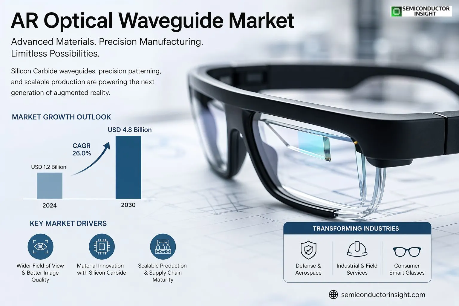
Inside AR Optical Waveguide Market the Shift from Glass Etching to Silicon Carbide Wafers
AR Optical Waveguide Market refers to the global ecosystem involved in the design, development, manufacturing, and integration of optical waveguide components used in augmented reality (AR) devices. These waveguides are transparent optical elements that guide and project digital images from a micro-display into the user’s field of view, allowing virtual content to blend seamlessly with the real world.
For the better part of a decade, the augmented reality industry has suffered from a massive identity crisis. The software was ready, the AI use cases were compelling, but the hardware specifically the lenses felt like they were designed by people who had never worn glasses.
The Silicon Carbide Disruption Entering the Chat
- The biggest story currently unfolding involves a material rarely discussed outside of high-power electronics: Silicon Carbide (SiC). Traditionally, waveguides have been made from glass or polymers with a refractive index hovering around 2.0.
- This sounds technical, but it translates directly to a hard physical limit: you generally cannot get a field of view beyond 30 or 40 degrees without severe color distortion or edge vignetting (where the corners of the image go dark).
- Goeroptics recently blew this limit out of the water at the SPIE AR|VR|MR conference. By switching to a SiC substrate with a refractive index of 2.65, they demonstrated the F50Se module.
- This is a full-color waveguide that achieves a 50-degree field of view without the usual optical artifacts.
- The engineering trade-off here is fascinating because SiC is incredibly hard and chemically stable.
- You cannot just stamp it with nanoimprint lithography like you would a soft polymer. Instead, manufacturers are being forced to adopt ion beam etching (IBE), a process borrowed from semiconductor fabrication, to carve the gratings into the wafer.
- This shift means that the foundries capable of making SiC chips for EVs are now becoming the default suppliers for AR optics.
From Production Struggles to Consistent Delivery
While new materials grab headlines, the quiet revolution is happening in how these wafers are patterned. For years, one of the biggest headaches has been full-color expansion. A single waveguide usually struggles to handle red, green, and blue light simultaneously because each color bends differently.
To solve this, engineers have turned to multiplexing. This is not just a buzzword; it is a structural change. We are seeing spatial multiplexing (popularized by HoloLens 2 with their butterfly grating structure) where different physical areas of the lens handle different colors. However, this requires extremely precise stitching of the gratings. If the alignment is off by even a few nanometres, the image misaligns. Magic Leap is pushing a different route with their proprietary jet and flash imprint lithography (JFIL). Unlike traditional etching that grinds away material, JFIL is an additive 3D patterning process. It allows them to create complex 3D structures in a single step. They recently signed a major agreement with Pegatron (the Taiwanese manufacturing giant) to ramp this process up. This is crucial because it validates that these complex, high-precision optics can leave the university cleanroom and hit the high-volume production lines.
To Stay Tuned with More meaningful and In-Depth Insights, Do Visit here: https://semiconductorinsight.com/report/ar-optical-waveguide-market/
The Defence Foundation and the Consumer Dream
- It is easy to get caught up in consumer smart glasses, but the current liquidity in this market is coming from the defence and aerospace sector.
- Vuzix, a veteran in the space, recently shipped a follow-on six-figure production order for waveguide-based display systems to a major US defence contractor. This is a significant signal. Defence applications demand ruggedization and high brightness.
- They do not care as much about fashion, but they do care about reliability in high-temperature, high-shock environments.
- This defence money is de-risking the supply chain. The waveguides going into fighter pilot helmets today are the same fundamental technology that will end up in ski goggles or field-service repair glasses tomorrow.
- The difference is the durability of the coating and the adhesive used to laminate the layers. Because Vuzix is fulfilling these military contracts, they have the cash flow to develop consumer-facing reference designs, like the prescription-ready waveguide they showcased with Himax at CES 2026.
- This design is only 0.35mm thick and supports high-index glass options, making it one of the first waveguides that actually looks like a lens rather than a block of acrylic.
Where the Semiconductor Supply Chain Fits?
We must look at this as a semiconductor supply chain issue. The production of AR waveguides is now moving from nanoimprint (stamping) back toward lithography (etching) as resolution requirements tighten. For high-end waveguides, manufacturers are using deep UV lithography tools to write the nanometer-scale gratings. This means the same fabs that make smartphone processors are now being asked to make pieces of glass.

Comments (0)