Optical Waveguide Glass Wafer Market Insights
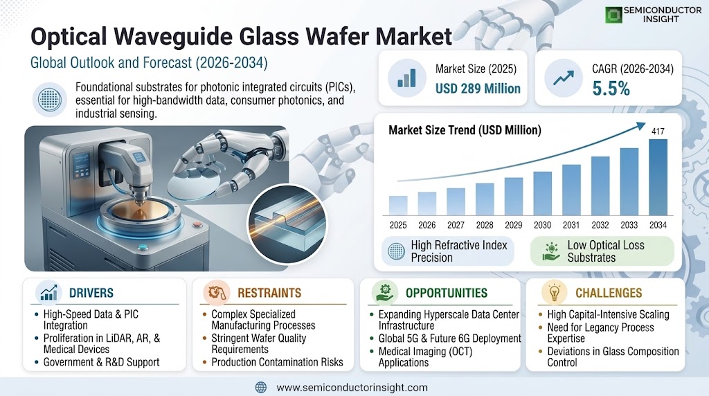
Optical Waveguide Glass Wafer market size was valued at USD 289 million in 2025. The market is projected to grow from USD 305 million in 2026 to USD 417 million by 2034, exhibiting a CAGR of 5.5% during the forecast period.
The Optical Waveguide Glass Wafer is a high-precision glass substrate specifically engineered for augmented reality (AR) and mixed reality (MR) optical waveguide systems. Serving as the core carrier for light propagation and image projection, this advanced substrate delivers high transmittance, lightweight construction, and superior optical performance. By integrating micro- and nano-structured surfaces, the wafer efficiently guides and controls light while minimizing optical loss and distortion, ensuring image clarity and immersive experience in wearable devices. In 2024, global production reached approximately 5 million pieces, with an average unit price of USD 60 per piece, an annual capacity per production line of around 20,000 pieces, and an average gross margin of approximately 49%. Key glass material and substrate suppliers in the upstream segment include DISCO, Lapmaster, SCHOTT, and Hoya, while downstream demand is primarily driven by AR and MR device manufacturers such as Apple, Microsoft, and Magic Leap.
The market is experiencing steady growth driven by the rapid expansion of the AR and MR industries across applications including gaming, enterprise training, remote collaboration, and industrial design. Continuous advancements in glass material quality, nanofabrication precision, and integration with complementary optical components are further enabling manufacturers to meet increasingly stringent requirements for optical clarity, durability, and scalable manufacturability. These factors, combined with rising adoption of wearable display technologies globally, are expected to sustain momentum throughout the forecast period.
MARKET DRIVERS
Rising Demand for High-Speed Data Transmission and Advanced Photonic Integration
optical waveguide glass wafer market is experiencing robust momentum, largely driven by the accelerating demand for high-bandwidth, low-latency data transmission across global telecommunications and data center infrastructure. As hyperscale data centers scale their operations to support cloud computing, artificial intelligence workloads, and edge computing deployments, the need for efficient optical interconnect solutions has intensified. Optical waveguide glass wafers serve as foundational substrates in photonic integrated circuits (PICs), enabling precise light guidance with minimal signal loss , a critical requirement in modern fiber-optic communication systems. The expanding deployment of 5G networks and the anticipated rollout of next-generation 6G architectures further underscore the strategic importance of this technology.
Proliferation of Photonic Integrated Circuits in Consumer and Industrial Electronics
Beyond telecommunications, the integration of photonic components into consumer electronics, medical imaging systems, and industrial sensing platforms is reshaping demand dynamics within optical waveguide glass wafer market. Sectors such as LiDAR-based autonomous vehicles, augmented reality (AR) headsets, and optical coherence tomography (OCT) devices in healthcare are increasingly incorporating waveguide-based optical components that require precision-engineered glass substrates. The superior refractive index uniformity, thermal stability, and low hydroxyl (OH) content of specialty optical glass wafers make them indispensable in applications where signal integrity and dimensional precision are non-negotiable.
➤ optical waveguide glass wafer market is strategically positioned at the convergence of photonics, semiconductor manufacturing, and advanced materials science , creating a uniquely resilient demand profile that spans consumer, industrial, and defense end-use segments.
Government-backed investments in photonic research and national semiconductor strategies across regions including the United States, European Union, Japan, and South Korea are further catalyzing market expansion. Initiatives aimed at reducing dependence on electronic integrated circuits by transitioning toward silicon photonics and hybrid glass-silicon platforms are creating long-term procurement pipelines for optical waveguide glass wafer manufacturers. This policy-level tailwind, combined with sustained private sector R&D investments, positions the market for durable structural growth over the medium-to-long term horizon.
MARKET CHALLENGES
Complex Manufacturing Processes and Stringent Substrate Quality Requirements
The fabrication of optical waveguide glass wafers involves highly specialized processes, including chemical vapor deposition (CVD), flame hydrolysis deposition (FHD), and ion exchange techniques, all of which demand exceptional process control and contamination-free environments. Achieving the requisite refractive index profiles, surface flatness tolerances within nanometer ranges, and low birefringence characteristics consistently across production batches presents significant technical challenges. Even minor deviations in glass composition or thermal treatment protocols can result in elevated optical losses, rendering wafers unsuitable for high-performance photonic applications. These constraints drive up production costs and create meaningful barriers to capacity scaling, particularly for emerging market entrants lacking legacy process expertise.
Other Challenges
Supply Chain Concentration and Raw Material Vulnerabilities
The optical waveguide glass wafer supply chain is exposed to geographic concentration risks, as the production of high-purity silica glass and specialty dopants such as germanium dioxide and rare earth oxides is concentrated among a limited number of global suppliers. Geopolitical tensions, trade restrictions, and logistics disruptions can introduce procurement uncertainties that downstream photonic device manufacturers find increasingly difficult to absorb. This structural vulnerability in the supply chain represents an ongoing challenge for market participants seeking to maintain cost predictability and delivery consistency.
High Capital Expenditure and Extended Technology Qualification Cycles
Establishing or upgrading manufacturing facilities capable of producing optical waveguide glass wafers to semiconductor-grade specifications requires substantial capital investment in cleanroom infrastructure, precision deposition equipment, and advanced metrology systems. Furthermore, qualification and certification cycles for new wafer substrates within photonic device supply chains can extend over multiple years, delaying revenue realization for manufacturers and creating adoption friction for innovative glass formulations despite demonstrated technical advantages.
MARKET RESTRAINTS
Competition from Silicon Photonics and Alternative Substrate Technologies
One of the most consequential restraints facing optical waveguide glass wafer market is the growing competitiveness of silicon-on-insulator (SOI) platforms and polymer-based waveguide technologies, which offer certain integration advantages within CMOS-compatible fabrication environments. Silicon photonics, in particular, benefits from the mature semiconductor manufacturing ecosystem, enabling cost-effective mass production of photonic components that partially overlap with glass waveguide applications. While glass substrates retain superior performance in low-loss, wide-bandwidth, and thermally demanding scenarios, the economic scalability of silicon-based alternatives continues to exert downward pressure on market penetration rates in certain application segments.
Cost Sensitivity in Price-Competitive End-Use Markets
In consumer electronics and certain telecommunications segments where procurement decisions are heavily influenced by unit economics, the relatively higher cost structure of precision optical waveguide glass wafers compared to standard substrates creates adoption barriers. Original equipment manufacturers (OEMs) operating under margin pressure may opt for lower-cost waveguide solutions that sacrifice some optical performance in favor of improved cost-per-unit metrics. This dynamic is particularly evident in high-volume, commodity-oriented deployment scenarios, where the performance premium of specialty glass wafers does not always translate into a justifiable total cost of ownership advantage at scale.
MARKET OPPORTUNITIES
Expansion of Quantum Photonics and Next-Generation Sensing Applications
The emergence of quantum computing and quantum communication platforms represents a compelling long-term growth opportunity for optical waveguide glass wafer market. Quantum photonic systems require ultra-low-loss optical waveguides with exceptional phase stability and minimal environmental sensitivity , performance characteristics that advanced specialty glass wafer platforms are uniquely positioned to deliver. Research institutions and quantum technology companies are actively evaluating glass-based photonic substrates for the development of quantum key distribution (QKD) modules, entangled photon sources, and photonic quantum processors, opening a differentiated demand channel that is structurally insulated from the cost pressures affecting conventional photonics markets.
Growing Adoption in Medical Imaging, Biosensing, and Wearable Optical Devices
The medical technology sector presents an increasingly significant opportunity for optical waveguide glass wafer manufacturers, as minimally invasive diagnostic tools, endoscopic imaging systems, and wearable biosensors continue to evolve toward higher optical performance thresholds. Applications including optical coherence tomography, fluorescence-based biosensing, and lab-on-chip diagnostic platforms require precisely engineered waveguide substrates capable of operating across specific wavelength ranges with high dimensional accuracy. As healthcare providers and medtech developers prioritize optical solutions that offer biocompatibility, chemical inertness, and long-term stability, specialty glass wafers are well positioned to capture an expanded share of this high-value application space over the forecast period.
Strategic Localization Initiatives and Regional Manufacturing Investments
National photonics and semiconductor localization strategies being pursued across North America, Europe, and the Asia-Pacific region are creating meaningful near-term and medium-term market opportunities for optical waveguide glass wafer producers. As governments prioritize supply chain resilience and domestic manufacturing capability in critical photonic components, publicly funded grants, tax incentives, and co-investment programs are lowering the financial barriers to capacity expansion for qualified manufacturers. Companies that proactively align their production footprint with regional procurement preferences and national technology priorities are well positioned to secure long-term supply agreements and establish competitive moats within the evolving optical waveguide glass wafer market landscape.
MAIN TITLE HERE () Trends
Rising Adoption of AR and MR Technologies Fueling Demand for Optical Waveguide Glass Wafers
optical waveguide glass wafer market is experiencing sustained growth momentum, primarily driven by the accelerating adoption of augmented reality (AR) and mixed reality (MR) technologies across a wide range of industries. As AR and MR devices become increasingly embedded in applications such as industrial training, remote collaboration, gaming, and engineering design, the demand for high-performance optical waveguide glass wafers continues to intensify. These precision glass substrates serve as the foundational carrier for light propagation and image projection within wearable AR/MR systems, making their optical quality and structural precision critical to overall device performance. In 2024, global production of optical waveguide glass wafers reached approximately 5 million pieces, underscoring the scale at which manufacturers are responding to downstream demand from device makers including leading technology firms across consumer and enterprise segments.
Other Trends
Advancements in Glass Material Quality and Nanofabrication Precision
A significant trend shaping optical waveguide glass wafer market is continuous innovation in upstream glass material quality and midstream nanofabrication processes. Manufacturers are investing in high-purity optical glass formulations , including lanthanum-based, phosphate-based, and silicate-based glass types , to achieve superior transmittance, minimal optical loss, and enhanced durability. Precision cutting, polishing, and nano-structured surface integration are increasingly critical process stages, directly influencing optical efficiency and production yield. The ability to manufacture wafers with varying refractive indices and controlled thickness profiles is becoming a key competitive differentiator, enabling device makers to achieve compact form factors, wider fields of view, and improved image clarity in next-generation wearable platforms.
Vertical Integration and Supply Chain Optimization Among Key Players
Another prominent trend in optical waveguide glass wafer market involves strategic efforts by leading manufacturers to strengthen supply chain resilience and optimize production economics. With an average gross margin of approximately 49% reported in 2024 and an average unit price of around 60 USD per piece, producers are under pressure to balance quality output with cost efficiency. Companies across the industrial chain , from upstream optical glass substrate suppliers to midstream precision processors , are increasingly pursuing tighter coordination to reduce lead times, improve yield rates, and meet the stringent optical inspection standards required by downstream AR and MR device integrators.
Integration with Advanced Optical Components Driving Product Innovation
optical waveguide glass wafer market is also being shaped by the growing need for seamless integration of waveguide glass wafers with other advanced optical components such as diffractive optical elements, holographic gratings, and micro-lens arrays. As device architectures become more sophisticated, the waveguide glass wafer must meet increasingly stringent specifications for surface flatness, refractive index uniformity, and coating compatibility. This trend is pushing manufacturers toward closer collaboration with downstream AR and MR device developers, fostering co-innovation models that accelerate product development cycles while ensuring that optical performance standards align with evolving end-use requirements across both consumer and enterprise applications.
COMPETITIVE LANDSCAPE
Key Industry Players
Optical Waveguide Glass Wafer Market: Competitive Dynamics and Leading Manufacturer Profiles
Optical Waveguide Glass Wafer market, valued at approximately USD 289 million in 2025 and projected to reach USD 417 million by 2034 at a CAGR of 5.5%, is characterized by a moderately consolidated competitive landscape dominated by a handful of highly specialized glass substrate and precision optics manufacturers. SCHOTT AG stands out as one of the foremost players, leveraging its decades-long expertise in specialty glass production to deliver high-purity, high-transmittance optical waveguide substrates optimized for augmented reality and mixed reality applications. Hoya Corporation similarly holds a prominent market position, backed by its advanced optical glass formulation capabilities and vertically integrated manufacturing infrastructure. These leading companies invest heavily in nanofabrication precision, surface polishing technologies, and proprietary coating processes to maintain competitive differentiation. The upstream segment of the industrial chain is particularly critical, as the quality of high-purity glass materials directly determines optical performance, yield rates, and ultimately the user experience in AR/MR wearable devices served by downstream OEMs such as Apple, Microsoft, and Magic Leap.
Beyond the tier-one incumbents, a number of specialized and regionally significant players are actively shaping the competitive dynamics of optical waveguide glass wafer market. Companies such as Corning Incorporated and AGC Inc. bring strong materials science capabilities and global manufacturing scale, enabling them to address increasing demand across lanthanum-based, phosphate-based, and silicate-based glass wafer segments. Emerging mid-tier manufacturers, particularly in East Asia, are gaining traction by offering competitive pricing structures while advancing their precision cutting, polishing, and optical inspection capabilities. DISCO Corporation, known for its precision dicing and grinding technologies, plays a vital role in the midstream processing segment, contributing to improved wafer yield and dimensional accuracy. As the AR/MR device ecosystem expands across gaming, industrial design, remote collaboration, and training verticals, competitive pressure is intensifying around throughput capacity , with an industry average annual capacity of approximately 20,000 pieces per production line , as well as around gross margin optimization, which currently averages around 49% across the sector. Innovation in nano-structured surface engineering and integration with other optical components remains a key battleground for sustained competitive advantage.
List of Key Optical Waveguide Glass Wafer Companies Profiled
- SCHOTT AG
- Hoya Corporation
- Corning Incorporated
- AGC Inc.
- DISCO Corporation
- Lapmaster International
- Ohara Inc.
- Nikon Corporation
- Nippon Electric Glass Co., Ltd.
- Sydor Optics
- Jenoptik AG
- II-VI Incorporated (Coherent Corp.)
- Photon Dynamics (Orbotech)
- LightPath Technologies
- Lens Technology Co., Ltd.
Segment Analysis:
| Segment Category | Sub-Segments | Key Insights |
| By Type |
|
Lanthanum-Based Glass Type holds a dominant position in optical waveguide glass wafer market owing to its exceptional optical properties that are critical for high-performance AR and MR applications.
|
| By Application |
|
Augmented Reality (AR) Devices represent the leading application segment, driven by surging consumer and enterprise adoption of AR headsets and smart glasses worldwide.
|
| By End User |
|
Consumer Electronics Manufacturers are the dominant end users of optical waveguide glass wafers, reflecting the rapid scaling of AR and MR product lines across major global technology brands.
|
| By Refractive Index |
|
High Refractive Index (above n1.9) glass wafers are the leading sub-segment, as they enable thinner waveguide architectures critical for compact and lightweight AR/MR wearable devices.
|
| By Thickness |
|
Ultra-Thin (below 0.3 mm) optical waveguide glass wafers are gaining strong traction as the leading thickness segment, aligned with the overarching industry goal of miniaturization in AR and MR device design.
|
Regional Analysis: Optical Waveguide Glass Wafer Market
Asia-Pacific
Asia-Pacific’s optical waveguide glass wafer manufacturing ecosystem is among the most vertically integrated globally. The region hosts specialized raw material suppliers, precision glass forming facilities, and cleanroom-grade processing units within close geographic proximity. This clustering effect reduces lead times, lowers logistics costs, and enables rapid iteration between material development and device fabrication , creating a compounding competitive advantage that is difficult for other regions to replicate in the near term.
Innovation in the Asia-Pacific Optical Waveguide Glass Wafer Market is propelled by robust collaboration between university research centers, national laboratories, and private enterprises. Japan’s photonics institutes and China’s state-sponsored semiconductor programs are actively developing next-generation waveguide architectures. Regional players are investing in ultra-thin wafer technologies and surface nano-structuring methods that enhance optical coupling efficiency and broaden application compatibility across telecom and AR/VR platforms.
The region’s voracious appetite for advanced consumer electronics, 5G network infrastructure, and data center optical interconnects is a primary catalyst for optical waveguide glass wafer consumption. Rapidly expanding augmented reality device pipelines from regional hardware developers in China, South Korea, and Japan are creating sustained procurement demand. Additionally, growing fiber-optic network rollout programs across Southeast Asia are broadening the addressable market for waveguide-based passive optical components.
Government initiatives across Asia-Pacific are directly reinforcing the optical waveguide glass wafer supply chain. China’s semiconductor self-sufficiency programs, Japan’s photonics industry roadmaps, and South Korea’s strategic material investment funds collectively create a supportive environment for capacity expansion. These policy frameworks lower barriers for domestic producers, attract foreign technology partnerships, and ensure a steady pipeline of skilled optical engineering talent through targeted educational investments.
North America
North America represents a highly significant and technologically sophisticated segment of Optical Waveguide Glass Wafer market. The United States serves as the primary growth engine, underpinned by a dense concentration of photonics companies, defense and aerospace optical system integrators, and world-class research universities advancing integrated photonics science. Demand from hyperscale data center operators seeking high-bandwidth optical interconnect solutions remains a consistent pull factor. The region also benefits from strong activity in LiDAR systems for autonomous vehicles, medical imaging waveguide applications, and next-generation AR/VR headset development. Canada contributes through its quantum photonics research capabilities. While North America relies partly on Asia-Pacific for substrate supply, domestic value-added processing and device integration capabilities are well established. Federal investment in photonic integrated circuit research through programs supporting domestic semiconductor supply chains further reinforces the region’s strategic importance in the optical waveguide glass wafer ecosystem through 2034.
Europe
Europe occupies a strategically important position in optical waveguide glass wafer market, characterized by deep expertise in precision optics, specialty glass manufacturing, and photonic integration research. Germany, the Netherlands, and France are central hubs of optical technology development, with established industrial players and research consortia driving innovation in waveguide substrate quality and functional coatings. European demand is strongly influenced by industrial automation, medical diagnostics, and aerospace sensing applications, all of which require high-reliability optical waveguide components. The region’s emphasis on sustainability and precision manufacturing aligns well with emerging requirements for energy-efficient photonic systems. European Union-funded research programs supporting photonic integrated circuits and quantum communications are creating additional long-term demand stimuli, ensuring that the region maintains a steady and technically progressive role in Optical Waveguide Glass Wafer market landscape through the forecast period.
North America (United States Focus)
Within the broader North American context, the United States specifically commands attention as a global center for optical waveguide glass wafer application development and systems integration. Silicon Valley and research corridors in Massachusetts and New York State host dense clusters of photonics startups and established optical component suppliers actively engaged in waveguide-based product development. Defense procurement programs requiring advanced electro-optic systems have historically driven specialty glass wafer demand, and this trend continues to evolve with sensor miniaturization and directed energy technology programs. The commercial sector, led by cloud computing infrastructure expansion and growing AR wearable device pipelines, is increasingly complementing defense-driven demand, broadening the total addressable market for optical waveguide glass wafers across the United States through the 2026–2034 outlook period.
Middle East & Africa
The Middle East and Africa region represents an emerging and gradually developing segment of Optical Waveguide Glass Wafer market. While domestic manufacturing capabilities remain nascent, several Gulf Cooperation Council nations are investing substantially in digital infrastructure modernization, including fiber-optic network expansion and smart city development , both of which generate downstream demand for optical waveguide components. The United Arab Emirates and Saudi Arabia are emerging as regional technology investment hubs, with strategic visions emphasizing advanced telecommunications and photonics adoption. Africa’s participation remains largely import-dependent, but growing mobile broadband infrastructure projects are establishing foundational demand. As international photonics suppliers seek geographic diversification and access to emerging economies, the Middle East and Africa region is expected to demonstrate gradual but meaningful market participation in optical waveguide glass wafer market over the medium to long term.
Report Scope
This market research report provides a comprehensive analysis of optical waveguide glass wafer market, covering the forecast period 2026–2034. It offers detailed insights into market dynamics, technological advancements, competitive landscape, and key trends shaping the industry.
Key focus areas of the report include:
- Market Overview: The report begins with an overview outlining its current market scenario, key growth indicators, and industry transformation drivers. It discusses macroeconomic factors, demand–supply balance, regulatory landscape, and the strategic role of optical waveguide glass wafers in powering advancements across industries such as augmented reality, mixed reality, consumer electronics, and industrial automation.
- Market Size & Forecast: Historical data and future projections for revenue, unit shipments, and market value across major regions and segments.
- Segmentation Analysis: Detailed breakdown by product type, refractive index, thickness, application, and end-user industry to identify high-growth segments and investment opportunities.
- Regional Insights: Insights into market performance across North America, Europe, Asia-Pacific, Latin America, and the Middle East & Africa, including country-level analysis where relevant.
- Competitive Landscape: Profiles of leading market participants, including their product offerings, R&D focus, manufacturing capacity, pricing strategies, and recent developments such as mergers, acquisitions, and partnerships.
- Technology Trends & Innovation: Assessment of emerging technologies, integration of micro- and nano-structured surfaces, nanofabrication precision techniques, fabrication methods, and evolving industry standards.
- Market Drivers & Restraints: Evaluation of factors driving market growth along with challenges, supply chain constraints, regulatory issues, and market-entry barriers.
- Stakeholder Insights: Insights for component suppliers, OEMs, system integrators, investors, and policymakers regarding the evolving ecosystem and strategic opportunities.
Primary and secondary research methods are employed, including interviews with industry experts, data from verified sources, and real-time market intelligence to ensure the accuracy and reliability of the insights presented.
FREQUENTLY ASKED QUESTIONS:
What is the current market size of Optical Waveguide Glass Wafer Market?
-> Global Optical Waveguide Glass Wafer Market was valued at USD 289 million in 2025 and is expected to reach USD 417 million by 2034, growing at a CAGR of 5.5% during the forecast period.
Which key companies operate in Optical Waveguide Glass Wafer Market?
-> Key players include upstream manufacturers such as DISCO, Lapmaster, SCHOTT, and Hoya, along with downstream application companies such as Apple, Microsoft, and Magic Leap, among others.
What are the key growth drivers?
-> Key growth drivers include rapid expansion of the AR and MR industries, rising demand in gaming, training, remote collaboration, and industrial design, as well as continuous innovation in glass material quality, nanofabrication precision, and integration with other optical components.
Which region dominates the market?
-> Asia-Pacific is the fastest-growing region driven by strong manufacturing capabilities and technology adoption, while North America remains a significant market owing to the presence of leading AR/MR device companies such as Apple, Microsoft, and Magic Leap.
What are the emerging trends?
-> Emerging trends include advanced micro- and nano-structured surface integration, high-refractive-index glass innovation, lightweight and compact waveguide designs, and the growing adoption of optical waveguide glass wafers in next-generation AR/MR wearable devices targeting wide field-of-view and high optical efficiency.

Get Sample Report PDF for Exclusive Insights
Report Sample Includes
- Table of Contents
- List of Tables & Figures
- Charts, Research Methodology, and more...
 Download Sample Report PDF