
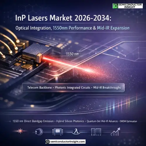
InP Laser Innovation Redefining Photonic Integration and Next-Gen Light Sources
Indium Phosphide (InP) lasers occupy a unique niche in semiconductor photonics because of their ability to emit efficiently at wavelengths crucial for telecom and sensing systems. InP is essential for laser sources used in fiber-optic networks and data centers because it permits direct band gap emission, like silicon, which is unable to produce light directly. This property also contributes to InP’s dominance in externally modulated lasers (EMLs) and continuous-wave (CW) lasers, which are essential for high-speed optical communication architecture.
The material’s strong optical performance in the near-infrared spectrum, particularly around the 1550 nm window, is tightly linked to the physics of InP’s crystalline structure and band alignment. These lasers deliver high spectral purity, stable power output, and reliable operation over wide temperature ranges, factors that industrial engineers value especially in demanding environments.
Before Proceeding, Feel Free to Overlook Our Updated Report:
https://semiconductorinsight.com/report/inp-lasers-market-size/
Integrating InP Lasers Directly onto Photonic Platforms
Recent research has focused on integrating InP lasers into silicon nitride photonics, a trend that shows how mainstream silicon photonics is benefiting from III-V materials. In a notable collaborative project among Ghent University, IMEC, and Thales Research, scientists used micro-transfer printing to place mini InP gain sections on top of a silicon nitride waveguide platform.
This hybrid laser integration achieves efficient optical coupling and supports high-capacity communication systems, coherent sensing, and microwave photonics. By combining the optical advantages of InP with the maturity of silicon photonic infrastructure, this approach addresses two longstanding challenges: the need for compact, high-performance light sources and practical integration with large-scale photonic circuits.
Strategic Outlook for Mid Infrared InP Laser Technologies
A recent breakthrough from University College London introduces InAs/InP quantum-dot lasers operating in the mid-infrared band (~2 µm) with significantly lower threshold current densities than previous designs.
This advancement matters because traditional InP lasers have struggled to reach high performance in wavelengths beyond near-infrared due to high required driving currents and thermal limitations. The low threshold current recorded (118 A/cm² per layer) opens doors for cost-effective, high-efficiency mid-IR sources, which are valuable in environmental sensing, medical diagnostics, and spectroscopy.
In practical terms, this technology points toward compact, energy-efficient sensors capable of detecting molecular signatures in gases or biological tissues, potentially transforming applications where deep IR light interaction is critical.
Lumentum Boosts Production Capabilities in InP Laser Segment
Photonics industry leader Lumentum recently announced a significant investment in expanding its InP laser chip capacity, even amid quarterly revenue challenges. The focus is squarely on meeting rapidly growing demand for lasers and transceivers used in cloud services and increasingly in AI-centric data networks.
A major customer lined up for high-speed optical transceivers underlines how InP lasers power the backbone of next-generation optical links. Lumentum’s expansion is expected to boost baseline InP wafer fabrication capacity by over 40 % in the coming year, reflecting confidence in future demand despite short-term market fluctuations.
This real-world example shows how leading semiconductor firms are aligning production capabilities with evolving data throughput requirements a stark reminder that InP lasers are not a niche component but a core enabler in modern information infrastructure.
Interplay with Photonic Integrated Circuits (PICs)
Photonic integrated circuits (PICs) represent a paradigm shift in how light signals are generated, manipulated, and processed on a single chip platform. InP is one of the primary material systems for PICs because it supports both active and passive optical functions.
Unlike traditional discrete laser modules, integrated solutions can place sources, modulators, and detectors on the same substrate. For coherent optical links, this means significant improvements in power efficiency and system footprint. Additionally, the hybrid integration of InP with silicon photonics is driving advancements in complex optical transceivers and dense wavelength-division multiplexing (DWDM) systems.
While still a technical challenge, these merged platforms promise future devices that are lighter, more power-efficient, and better suited to intelligent edge and cloud systems a trend clearly supported by ongoing research and demonstration projects.
Diversified Application Opportunities across Industries
Though the largest segment for InP lasers remains fiber-optic communications, their application portfolio is expanding:
- LiDAR and Optical Sensing: High-speed, coherent sources are increasingly used in light detection and ranging systems, vital for autonomous navigation and environmental mapping.
- Biomedical Diagnostics: InP’s wavelength versatility enhances tools such as optical coherence tomography (OCT) and minimally invasive diagnostic lasers.
- Microwave Photonics: Combining photonic and RF systems for high-frequency signal processing benefits from stable, narrow-line width InP laser sources.
- Mid-Infrared Spectroscopy: As illustrated by quantum-dot advances, extending InP lasers into the 2 µm range opens more precise molecular sensing capabilities.
These applications showcase how InP laser technology is morphing from a telecom-centric technology to a multi-sector enabler.
Sustainability in InP Supply Chains and Material Use
Recent supply-chain analyses highlight a notable constraint in indium procurement, with lead times increasing substantially over the past few years. Recycling rates for indium the core raw material for InP remain low, intensifying production bottlenecks as demand grows across high-tech industries.
Addressing this requires both innovations in material recovery processes and alternative approaches such as better epitaxial growth techniques or hybrid material solutions. These efforts are becoming critical as the semiconductor ecosystem seeks to balance growth with more sustainable, resilient supply chains.
The next frontier for InP lasers involves deeper integration with photonic computing architectures, AI-optimized optical networks, and advanced sensing systems. As research continues to push into longer wavelengths and higher integration densities, we can expect novel platforms that leverage InP lasers not just as standalone light sources but as core functional blocks in heterogeneous photonic systems.
This ongoing evolution underscores a broader transformation: InP lasers are not merely components they are building blocks for tomorrow’s interconnected digital and sensing infrastructure. Their trajectory promises deeper impact across communications, diagnostics, and environmental technologies, reflecting a vibrant future for this semiconductor class.

Comments (0)