Inference AI Chips Market: The Semiconductor Engines Delivering Instant AI Intelligence
Inference AI chips represent a specialized class of semiconductors engineered to execute trained artificial intelligence models with remarkable speed and efficiency. Inference concentrates on applying those previously learned patterns to new inputs in real time, in contrast to the computationally demanding process of training neural networks, which necessitates large parallel computations across enormous datasets.
This shift in workload has driven semiconductor designers to prioritize low-latency execution, minimal power draw, and compact architectures that fit everything from data centre racks to pocket-sized edge devices. The result is silicon optimized for the moment-to-moment decisions that make AI feel instantaneous whether recognizing objects in a smartphone camera or recommending the next action in an autonomous system.
What Sets Inference Hardware Apart in Semiconductor Design
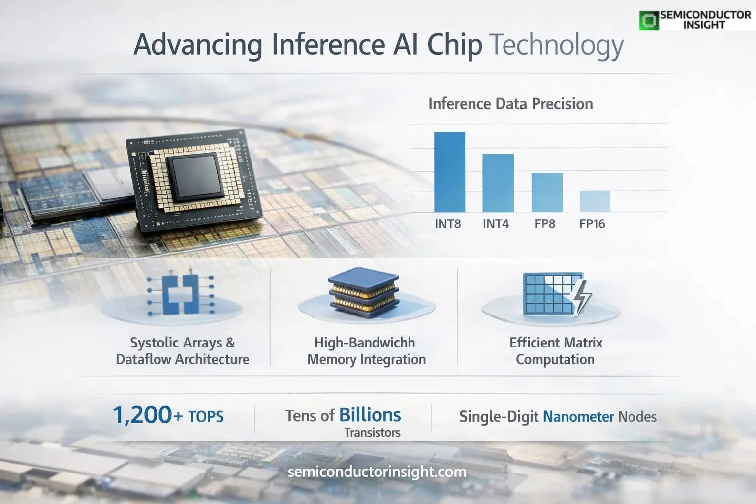
· At the architectural level, inference chips excel through many core and spatial computing layouts that handle low-precision arithmetic far more effectively than general-purpose processors.
· Operations typically run in INT8, INT4, or even novel formats like FP8 and FP16, slashing the computational overhead while preserving accuracy for most real-world tasks.
· These designs often incorporate systolic arrays or dataflow architectures that stream data directly through processing elements, minimizing memory trips and maximizing throughput. High transistor densities reaching tens of billions of MOSFETs in flagship designs enable this density of specialized cores without ballooning die size.
· The emphasis stays on inference-specific optimizations such as workload-aware throttling and efficient matrix multiplication blocks, which allow the chip to sustain trillions of operations per second under tight thermal and power budgets.
You Can Freely Surf Our Latest Updated Report Here: https://semiconductorinsight.com/report/inference-ai-chip-market/
Recent Semiconductor Breakthroughs Reshaping Inference Capabilities
Developments in 2025 and 2026 have accelerated these capabilities with striking real-world examples. NVIDIA’s Jetson T4000 module, built on the Blackwell architecture, delivers up to 1,200 FP4 sparse teraflops of AI compute alongside 64 GB of memory in a compact, power-efficient package tailored for robotics and edge applications. Its larger sibling, the Jetson T5000, pushes performance to 2,070 FP4 sparse teraflops while maintaining thermal envelopes suitable for deployment in industrial automation.
On the data-center front, Google’s latest Tensor Processing Unit iterations Trillium as TPU v6 and Ironwood as TPU v7 integrate native optimizations for agentic AI workflows, enabling faster reasoning loops and lower total cost of ownership through optical circuit switching. Google has also advanced its Coral NPU platform with a RISC-V-based reference implementation released in late 2025, offering an open, modular accelerator that developers can integrate across diverse edge hardware. Meanwhile, Microsoft’s Copilot+ PCs incorporate neural processing units rated at over 40 trillion operations per second, bringing on-device inference to everyday laptops for tasks like real-time image enhancement and local language processing.
The Fabrication Journey from Wafer to Inference Accelerator
Manufacturing these chips relies on cutting-edge semiconductor processes that balance density, power, and yield. Production begins in advanced fabrication facilities where extreme ultraviolet lithography patterns transistors at scales measured in single-digit nanometers.
Wafers undergo dozens of deposition, etching, and polishing steps before the dies are diced, tested, and packaged often with high-bandwidth memory stacks or chiplet interconnects for seamless data movement. Liquid-cooled assemblies and vertical stacking techniques, as seen in Google’s TPU v4 with its four high-bandwidth memory modules, allow dense integration without overheating. Post-fabrication validation includes rigorous electrical testing to confirm low-precision performance and power efficiency metrics, ensuring each chip meets the exacting demands of continuous inference workloads.
High-Bandwidth Memory and Precision Techniques Driving Efficiency
· A critical enabler for modern inference silicon is the integration of high-bandwidth non-volatile or stacked memory directly alongside the accelerator cores.
· This architecture keeps neural network weights readily accessible, eliminating bottlenecks during rapid forward passes through layered models.
· Techniques like layer fusion in compilers further optimize execution by combining sequential operations into single hardware passes, reducing data movement and boosting utilization rates.
· Power efficiency gains come from workload-aware designs that dynamically scale voltage and frequency, sometimes achieving tokens-per-watt improvements that make large language model inference practical even in constrained environments.
These semiconductor-level refinements rooted in co-design between hardware and software teams translate directly into smoother, more responsive AI experiences across applications.
Comments (0)