
imec Demonstrates Record WSe₂-Based 2D pFETs, Advancing the Future of Logic Scaling
At the IEEE International Electron Devices Meeting 2025 held in San Francisco from 6–10 December, imec, the world-renowned nanoelectronics research center, unveiled a major breakthrough in 2D transistor technology. The team reported record performance p-type field-effect transistors (pFETs) built with monolayer tungsten diselenide (WSe₂) channels, achieving drive currents as high as 690 µA/µm.
This milestone represents a significant step forward for 2D-material-based logic devices, which are widely viewed as a long-term solution for extending the semiconductor logic roadmap beyond the limits of silicon.
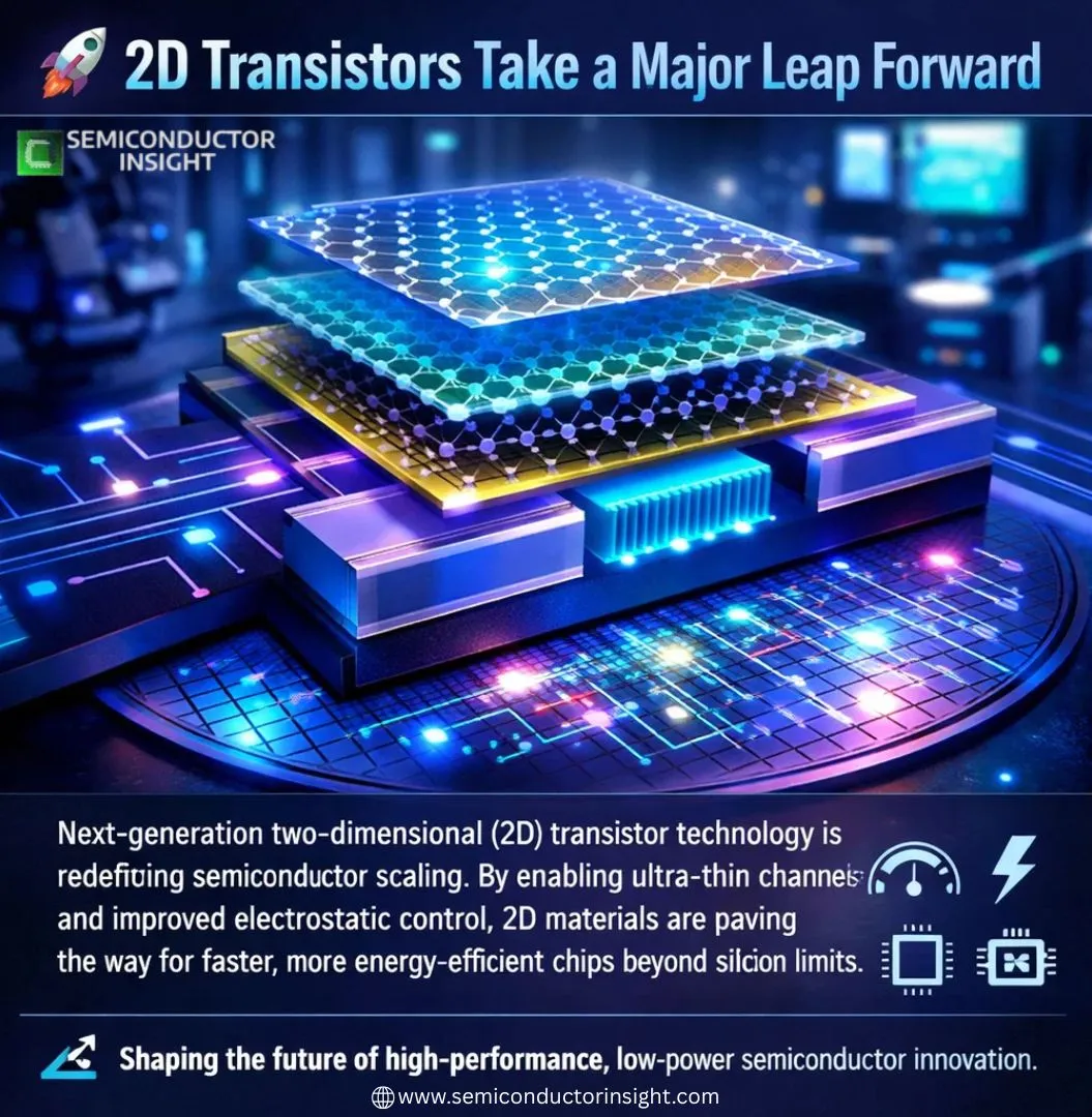
Why WSe₂ and 2D Materials Matter?
Replacing conventional silicon channels with atomically thin 2D transition-metal dichalcogenides (MX₂) offers clear advantages:
- Ultimate gate and channel length scaling
- Strong electrostatic control
- High carrier mobility even at extreme dimensions
While much of the industry’s focus has been on n-type devices using materials such as WS₂ and MoS₂, imec’s work highlights the growing importance of high-performance p-type devices, where materials like WSe₂ are essential.
Key Technical Advancements Highlighted at IEDM
imec’s results go beyond device performance and address critical manufacturing challenges required for large-scale adoption:
- High-quality 2D material integration compatible with advanced CMOS flows
- Improved source/drain contact modules enabling lower resistance
- Optimized gate stack integration for better device reliability
- Progress toward 300 mm fab compatibility, a key industry requirement
These developments were achieved through deep collaborations with leading semiconductor manufacturers within imec’s CMOS Industrial Affiliation Program (IIAP), combining manufacturer-supplied 2D material layers with imec’s optimized process modules.
Industry Impact
According to imec, these breakthroughs demonstrate that 2D pFET technology is moving closer to practical, manufacturable logic solutions, rather than remaining a purely academic concept. Balanced advances in both n-type and p-type devices are crucial for future CMOS architectures, making this work a pivotal contribution to next-generation chip design.
As logic scaling becomes increasingly complex, imec’s latest results reinforce the role of 2D materials as a credible path forward for post-silicon semiconductor technologies.
You Can Go Through Our Relevant Report Insights: https://semiconductorinsight.com/report/bio-fet-market/

Comments (0)