
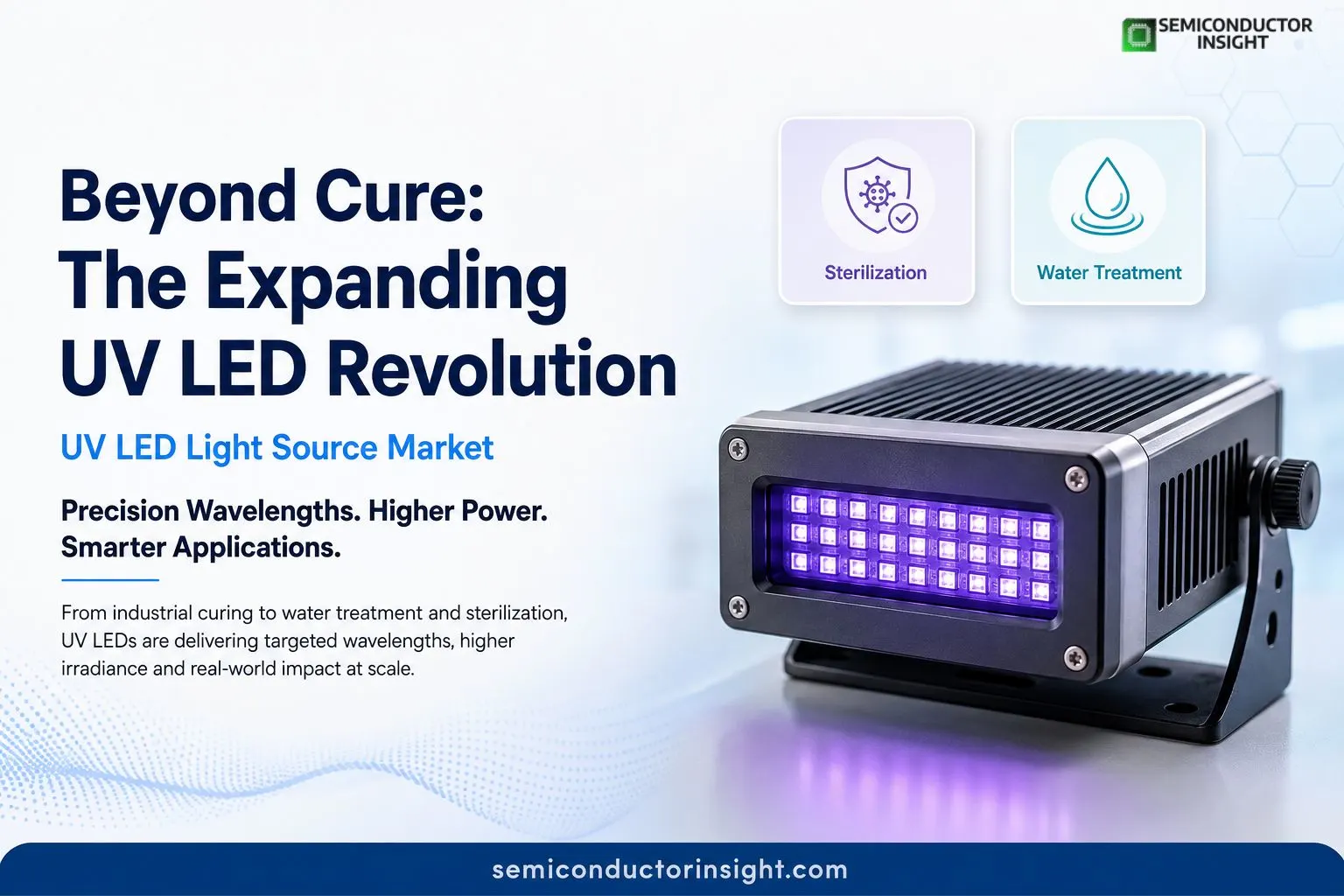
How Is UV LED light source market Changing in 2026? A Technology Focused Industry Breakdown
UV LED light source market is moving well beyond the image of a small ultraviolet lamp used for curing. Today, UV LEDs span UVA, UVB and UVC wavelengths, allowing manufacturers to engineer light sources for adhesives, coatings, printing, sterilization, sensing, water treatment and specialized scientific equipment.
The underlying semiconductor technology is equally diverse. Deep-ultraviolet LEDs generally rely on AlGaN-based materials, while longer-wavelength UVA devices can be engineered for high-output curing systems. Research on AlGaN deep-UV LEDs has demonstrated operation from approximately 210-280 nm, highlighting the broad spectral range available through semiconductor bandgap engineering.
Wavelength Is Becoming the Real Product Specification
For UV LED manufacturers, simply stating ‘UV output’ is no longer enough. The wavelength determines the application.
210-280 nm → Deep-UVC research and sterilization
275-280 nm → Disinfection and water treatment
365 nm → Specialized curing and photochemical processes
385-395 nm → Industrial curing and coatings
405 nm → Adhesives, printing and selected curing processes
Commercial curing systems now commonly offer 365, 385, 395 and 405 nm configurations, allowing manufacturers to match the emitted spectrum to the photoinitiator and substrate being processed.
Don’t Forget to Surf Our Updated Report for More Detailed Analysis: https://semiconductorinsight.com/report/uv-led-light-source-market-2/
The Power Density Race Has Moved Forward
Ø The important specification is increasingly irradiance rather than simply electrical input. Current industrial systems demonstrate how rapidly this parameter has advanced.
Ø Excelitas reports UV LED curing heads capable of reaching 22 W/cm² peak irradiance, with optical power up to 1,100 mW, while its newer controller architecture can operate multiple LED heads independently.
Ø Other industrial systems reach approximately 25 W/cm² at 385-405 nm, demonstrating how UV LED sources are being engineered for high-speed manufacturing rather than low-intensity laboratory illumination.
Ø This matters for production lines because higher irradiance can allow manufacturers to deliver the required UV dose in shorter exposure windows.
A Major 2026 Application Story Is Water
UVC LEDs are gaining attention in water treatment because they can be switched instantly, configured in compact arrays and designed around specific wavelengths.
A particularly important real-world demonstration involved a 280 nm UV LED wastewater reactor operating at flows of 545 and 817 m³ per day. The system achieved more than 3-log average reduction at the lower flow and more than 2.5-log reduction at the higher flow under the reported operating conditions. The reactor used an approximately 80 cm chamber and operated with residence times measured in seconds rather than minutes.
That example moves UV LED technology from laboratory experimentation toward genuine municipal-scale deployment.
The Efficiency Gap Is Narrowing Through Better Device Design
· Efficiency remains one of the most closely watched parameters in UVC LEDs. Earlier commercial 280 nm devices had relatively low wall-plug efficiency, but research and device engineering have produced significant improvements.
· One study reported that commercially available 280 nm UV LEDs had reached approximately 9-20.3% external quantum efficiency, compared with much lower levels reported in earlier generations.
· The same research found that a 280 nm LED could achieve comparable wastewater disinfection at a lower delivered fluence than the conventional system under the tested conditions.
· Recent AlGaN research has also demonstrated a 270 nm LED producing 140.1 mW optical output at 850 mA, with an external quantum efficiency reported at 4.5 times that of the researchers’ conventional reference device.
Electronics Manufacturing Is Driving another Growth Lane
UV LEDs are increasingly integrated into electronics manufacturing for adhesive curing, conformal coatings, component fixation and optoelectronic assembly. Modern area-curing equipment is designed around uniform irradiance across complete assemblies rather than exposing one small point at a time.
Current systems can deliver footprints such as 100 × 100 mm, while larger modular platforms can be extended to widths or lengths suitable for production lines. Some systems also provide optical-output stability of approximately ±5%, helping manufacturers maintain repeatable curing conditions.
The Semiconductor Opportunity Is Moving Deeper Into the Light Source
The next stage of UV LED light source market is increasingly connected to AlGaN material quality, quantum-well engineering, optical extraction, thermal management and wavelength-specific packaging.
The competitive question is therefore shifting from ‘Can an LED produce ultraviolet light?’ to ‘Can the semiconductor generate the required wavelength, optical power, efficiency and lifetime at industrial scale?’
That shift is opening a broader technology landscape in which a 270 nm deep-UV device, a 280 nm water-treatment module and a 395 nm industrial curing head may all belong to the same UV LED ecosystem but serve completely different engineering r

Comments (0)