

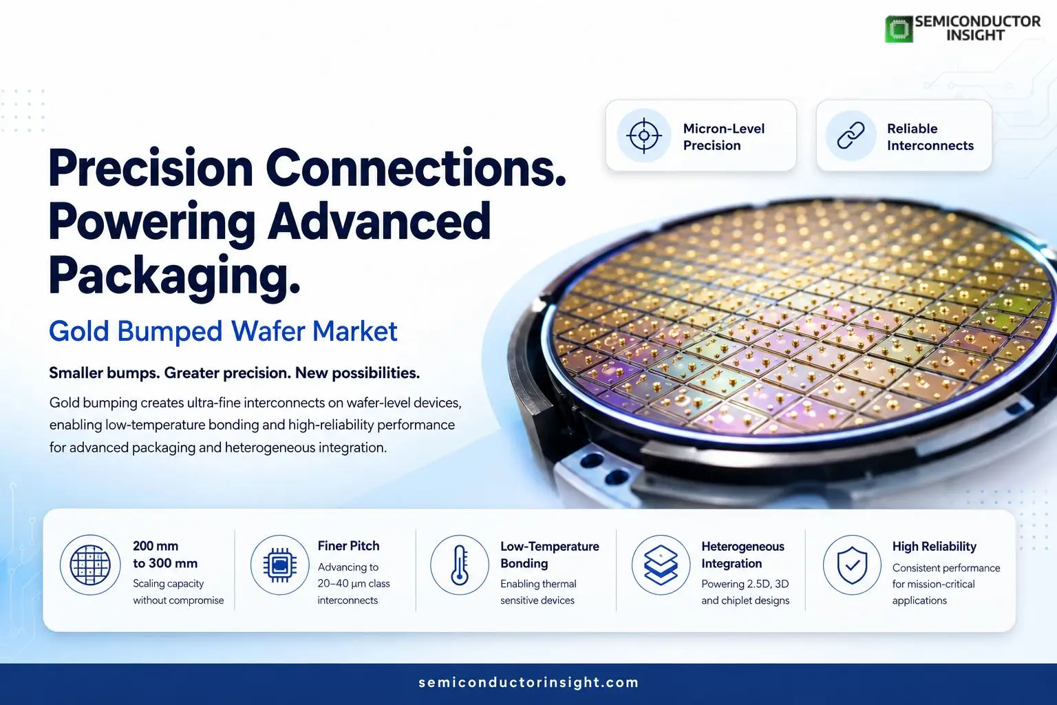
How Is Gold Bumped Wafer Market Changing in 2026? A New Look at Semiconductor Interconnect Technology
A semiconductor wafer can contain thousands of individual devices, but the electrical connection between those devices and their packages depends on structures measured in micrometers. Gold bumping occupies this highly specialized layer of semiconductor manufacturing by forming tiny gold-based interconnect structures directly on wafer-level devices.
Unlike conventional solder bumping, gold bumping is particularly associated with applications requiring fine, reliable electrical connections. Historical industry documentation identifies gold bumping as a wafer-level technology used especially for LCD and PDP driver IC packaging, while modern wafer-bumping platforms increasingly combine gold stud bumping with wafer bonding and heterogeneous integration.
The Process Starts Before the Bump Exists
Gold bump production is not simply a matter of depositing gold onto an exposed aluminum or copper pad. The wafer first requires suitable pad preparation and metallization, followed by bump formation, bonding or plating, inspection and subsequent assembly.
A simplified production chain is:
Processed wafer → pad preparation → UBM or bonding interface → Au bump formation → height and position inspection → wafer test → dicing → package assembly
The objective is consistent bump geometry across the wafer. Even small variations can affect contact resistance, bonding uniformity and package reliability when thousands of connections are assembled together.
200 mm Is Established While 300 mm Pushes Capacity
- Wafer diameter is becoming an important indicator of how bumping technology fits into high-volume semiconductor manufacturing.
- Amkor reports wafer-bumping capabilities covering both 200 mm and 300 mm wafers, including production-certified lead-free bumping technologies.
- Gold bumping equipment has also moved toward larger workpieces. At SEMICON Taiwan 2025, Kulicke & Soffa showcased wafer-level equipment capable of bonding wafers up to 300 mm, with stated placement accuracy of approximately ±5.0 μm at 3σ for 300 mm workpieces and low-temperature gold-bumping capability.
- That combination of 300 mm handling and micrometer-level placement illustrates where the technology is heading: larger wafers without sacrificing interconnect precision.
Why Gold Still Has a Place in the Interconnect Toolbox?
Copper has become increasingly important in advanced packaging because of its electrical and mechanical advantages. Amkor, for example, reports copper-pillar structures reaching 30 μm fine-pitch capability for selected configurations.
Gold, however, retains a distinct position where bonding characteristics, corrosion resistance, process compatibility and specialized low-temperature interconnection are important. Tohoku-MicroTec has been developing fine-pitch Au micro-bump technology for heterogeneous integration involving silicon, compound semiconductors and MEMS, including bonding processes at temperatures below 200°C.
This makes gold particularly interesting for devices where thermal exposure must be tightly controlled.
You Can Freely Surf Our Latest Updated Report Here: https://semiconductorinsight.com/report/gold-bumped-wafer-market/
The 40 μm Benchmark Shows Where Fine Pitch Is Going
Advanced packaging is steadily pushing interconnect dimensions downward. In an imec demonstration, automated probing was successfully performed on 40 μm-pitch micro-bump arrays across 300 mm wafers, with array sizes reaching 1,752 micro-bumps in one of the demonstrated configurations. The research team also investigated 20 μm-pitch probing.
These figures are important because bumping and probing cannot be considered independently. As bump pitch shrinks, manufacturers need corresponding improvements in alignment, inspection, probe technology and bonding accuracy.
Gold Bumping Finds a New Role in Heterogeneous Integration
The packaging landscape is changing from simply connecting one die to one substrate toward combining different chip types in a single package. Wafer-level technologies now support 2.5D, 3D, chiplet and heterogeneous-integration architectures.
Amkor’s wafer-level packaging portfolio includes wafer-level system-in-package and 3D package-stacking approaches, demonstrating how bumping technology is becoming part of increasingly complex integration flows.
The implication for Gold Bumped Wafer Market is significant: its relevance increasingly depends on whether gold interconnects can deliver the precision and thermal compatibility required by specialized multi-die architectures.
A New Packaging Equation for 2026
- The market is no longer defined simply by the number of gold bumps produced.
- The more useful indicators are wafer diameter, bump pitch, placement accuracy, bump height uniformity, bonding temperature, wafer-level yield and compatibility with heterogeneous integration.
200 mm production → 300 mm processing → finer pitch → lower-temperature bonding → multi-die integration → higher-density packages
Gold bumping is unlikely to replace every copper or solder interconnect. Instead, its opportunity is becoming more specialized: precision-driven semiconductor packaging where material properties and bonding conditions matter as much as electrical connectivity.

Comments (0)