
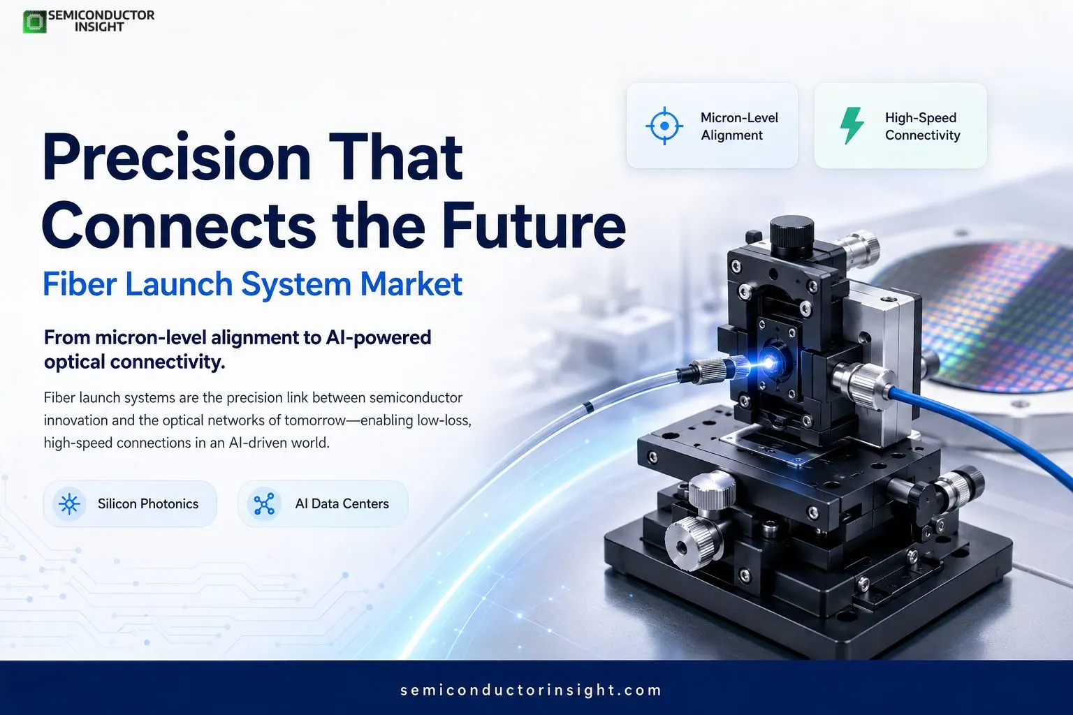
How Fiber Launch Systems Are Powering the Future of Silicon Photonics
The semiconductor industry is approaching a point where moving data can become just as important as processing it. Electrical interconnects remain dominant, but the rapid expansion of artificial intelligence infrastructure is pushing optical technologies closer to the processor. That shift puts unusual importance on a seemingly small manufacturing step: getting light into and out of an optical fiber with extremely high precision.
This is where fiber launch systems enter the photonics equipment chain. These systems position optical fibers against lasers, photodiodes, silicon-photonic devices, waveguides and other optical components while controlling alignment with microscopic precision. In semiconductor laboratories and production environments, the objective is simple but demanding: maximize optical coupling while minimizing insertion loss, instability and alignment time.
The Tiny Alignment Problem behind Massive Data Movement
A conventional electrical connection carries electrons through a conductive pathway. A photonic connection instead converts electrical information into optical signals, transports those signals through fiber or an integrated waveguide, and converts them again at the receiving side.
Electrical Signal
↓
Laser / Photonic Source
↓
Fiber Launch Alignment
↓
Optical Fiber
↓
Photonic Receiver
↓
Electrical Processing
The fiber-launch stage therefore becomes a critical interface between semiconductor fabrication and optical communication.
Modern systems may need to position fibers with micrometer-level accuracy, while some photonic alignment applications demand movement in multiple axes, including X, Y, Z and angular adjustment.
Silicon Photonics Is Changing What the Equipment Must Handle
- Silicon photonics has moved from research laboratories into commercial networking and data-center applications. Intel reported in 2024 that it had shipped more than 8 million silicon-photonics-based transceivers, illustrating the scale at which integrated photonics has already entered the communications ecosystem.
- The technology is becoming particularly important because conventional electrical interconnects face increasing power and bandwidth limitations as processors become more powerful. Optical connections can transport enormous amounts of information over fiber while reducing some of the transmission losses associated with long electrical pathways.
- For fiber launch equipment, this translates into a more complicated requirement: the system must work with increasingly small optical structures while maintaining repeatable coupling performance.
A Fiber Is No Longer Just a Cable Connection
The modern photonics assembly line can involve several different coupling geometries. Edge coupling connects optical fibers to waveguides at the side of a chip, while grating couplers allow light to enter or leave through the surface of the photonic device.
This distinction matters because each architecture creates a different alignment problem.
Edge Coupling
Fiber →→→ [Waveguide]
CHIP
Grating Coupling
Fiber
↓
↓↓↓↓↓
[Grating]
[PHOTONIC CHIP]
Equipment manufacturers are therefore developing increasingly flexible positioning platforms capable of handling different fiber arrays, photonic packages and optical components.
Explore the full report details in our recently refreshed edition anytime: https://semiconductorinsight.com/report/fiber-launch-system-market-2/
AI Data Centers Are Bringing Photonics Closer to the Chip
The extraordinary growth of AI accelerators is changing the economics of data movement. NVIDIA’s latest accelerated-computing platforms increasingly incorporate high-speed networking technologies, while hyperscale data-center operators continue expanding optical infrastructure.
The next major development is co-packaged optics, where optical engines move much closer to switching or computing silicon. Instead of treating optical transceivers as distant modules, manufacturers are investigating architectures where optical components sit alongside high-performance processors or switches.
For fiber launch systems, this creates a new precision requirement. Optical coupling can no longer be treated as a separate laboratory operation; it increasingly becomes part of advanced semiconductor packaging and automated production.
What the Next Equipment Generation Is Optimizing?
The most important equipment improvements are increasingly centered on repeatability, alignment intelligence and integration rather than simply increasing mechanical movement.
Modern platforms are being designed around:
- Multi-axis Nano positioning
- Automated optical-power optimization
- Machine-vision alignment
- Multi-fiber array handling
- Low-loss coupling measurement
- Software-controlled calibration
- High-throughput device characterization
These capabilities are particularly valuable for silicon photonics, optical transceivers, photonic integrated circuits and advanced optical packaging.
The Semiconductor Factory Is Becoming More Optical
The significance of fiber launch systems extends well beyond one equipment category. Semiconductor manufacturing is gradually incorporating lasers, optical waveguides, photonic integrated circuits and optical I/O into the same ecosystem that already contains advanced packaging, chiplets and high-bandwidth memory.
As AI accelerators move toward increasingly dense computing architectures, the bottleneck is shifting from simply building faster chips to connecting those chips efficiently. Fiber launch technology occupies one of the smallest physical points in that chain, but its role is becoming disproportionately important.
The industry’s direction is increasingly clear: more optical channels, tighter coupling tolerances, greater automation and shorter distances between photonics and compute. That combination is turning precision fiber-launch equipment from a specialized laboratory tool into an increasingly relevant component of next-generation semiconductor and photonics manufacturing.

Comments (0)