

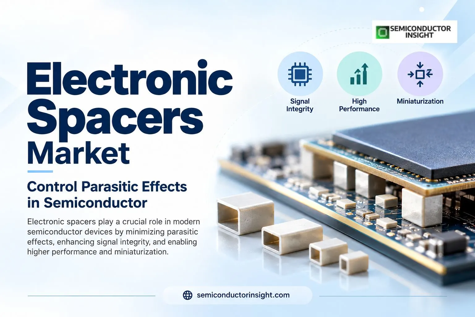
How Do Electronic Spacers Control Parasitic Effects in Semiconductor Devices? A Closer Look at Modern Chip Architecture
In advanced semiconductor manufacturing, a spacer is no longer simply a structure placed beside a transistor gate. At increasingly small dimensions, its dielectric properties, thickness and geometry can influence electrostatic control, parasitic capacitance, leakage and high-frequency behavior.
That makes spacer engineering increasingly relevant as manufacturers move from conventional FinFET structures toward gate-all-around and nanosheet architectures. Recent 2026 research has specifically examined how different spacer dielectric configurations affect advanced stacked nanosheet transistors. ScienceDirect
Nanosheets Are Changing What a Spacer Has to Do
- Gate-all-around architectures surround the conducting channel more completely than earlier transistor structures, improving electrostatic control as dimensions shrink.
- Intel’s current RibbonFET technology, for example, uses gate-all-around control around narrow silicon ribbons and is being developed for advanced computing applications.
- In such structures, the spacer sits within a much more tightly engineered three-dimensional environment. Its role therefore extends beyond physical separation; the material can affect the electrical interaction between neighboring regions of the transistor.
- This is one reason spacer materials are becoming an increasingly specialized part of advanced-node process development.
High-k and Low-k Materials Are Being Tested for Different Jobs
There is no universal spacer material that delivers the same advantage across every device architecture.
- A 2026 study comparing air, SiO₂, Si₃N₄ and HfO₂-based spacer configurations found that high-k spacers can support transistor scalability, while low-k structures can reduce parasitic capacitance in high-speed applications.
- The work also reported strong DC and RF characteristics from a Si₃N₄ plus HfO₂ configuration.
Another 2026 study on sub-5 nm TreeFET structures found HfO₂ favorable for digital performance, while a combination of HfO₂ and air produced advantages for RF performance through lower parasitic capacitance.
The message for process engineers is straightforward: spacer selection is increasingly becoming an optimization exercise rather than a simple materials choice.
The Dimensions Are Moving Into the Nanometer Range
The scale of the problem becomes clearer in advanced device research. Recent work on ultra-small vertical thin-film transistors investigated composite spacer structures approximately 20 nm thick and reported a reduction in leakage-current density of two orders of magnitude compared with single-layer spacer structures in the tested architecture.
At these dimensions, a small change in thickness, interface quality or dielectric constant can influence electrical behavior. Manufacturing consistency therefore becomes as important as the nominal material specification.
Our most recent updated related study is available for free at this link: https://semiconductorinsight.com/report/electronic-spacer-market/
Spacer Formation Is Becoming a Process-Integration Problem
The material itself is only one part of the equation. Deposition, etch selectivity, profile control and interface quality determine whether a designed spacer actually appears on the wafer as intended.
- Research published in 2026 examined vertical SiO₂ dielectric spacers for vertical gate-all-around MOSFET structures using inductively coupled plasma-enhanced chemical vapor deposition combined with wet etch-back.
- The study specifically addressed pit formation at the spacer-channel interface, which can affect device reliability.
This illustrates why spacer development increasingly involves cooperation between materials scientists, deposition specialists, etch engineers and device designers.
Advanced Packaging Is Expanding the Meaning of Spacer Engineering
The spacer story does not stop at the transistor.
As chiplets and vertically stacked dies become increasingly important for AI and high-performance computing, packaging structures also require carefully controlled mechanical and electrical spacing. Intel’s current advanced-packaging portfolio combines Foveros 3D stacking with EMIB technologies for heterogeneous multi-die systems.
TSMC is similarly expanding advanced packaging capacity, with its 2025 annual report stating that a 5.5-times mask/reticle-size CoWoS interposer was qualified and planned for volume production in 2026 to address AI and HPC requirements.
The broader implication is that spacing, isolation and dimensional control are becoming essential across both front-end device fabrication and back-end integration.
AI Chips Are Raising the Precision Requirement
The semiconductor industry reached $791.7 billion in global sales in 2025, according to the Semiconductor Industry Association, with the organization expecting worldwide sales to approach $1 trillion during 2026. Semiconductor Industry Association
Much of the current expansion is tied to logic and memory used in AI and data-center systems. Those applications are increasing pressure on transistor density, power efficiency, bandwidth and package-level integration.
That environment creates a direct technical incentive to refine every part of the device architecture, including structures that may occupy only a tiny portion of the transistor.
A New Role for Spacer Engineering
Electronic Spacer Market is increasingly connected to a semiconductor industry where the difference between a successful and unsuccessful device can be determined by structures measured in nanometers.
The next phase is likely to revolve around tighter dimensional control, alternative dielectric combinations, composite structures and process flows capable of producing reliable spacers in increasingly complex three-dimensional devices. Recent research already shows that spacer composition can influence DC, RF, leakage and scaling behavior. ScienceDirect
As GAA transistors, nanosheets, vertical devices and advanced chiplet architectures develop together, the spacer is becoming less of a supporting feature and more of an engineered element in the semiconductor device itself.

Comments (0)